Semiconductor device with double barrier film

a technology of barrier film and semiconductor, applied in the direction of semiconductor device, semiconductor/solid-state device details, electrical apparatus, etc., can solve the problems of deteriorating device reliability, disadvantageous fine patterning, and difficult to microfabricate contacts by so-called lithography technology

Inactive Publication Date: 2006-07-18
KK TOSHIBA
View PDF6 Cites 20 Cited by
  • Summary
  • Abstract
  • Description
  • Claims
  • Application Information

AI Technical Summary

Problems solved by technology

Furthermore, with the progress of the generation of cells, it becomes difficult to carry out microfabrication of contacts by so-called lithography technology.
Consequently, the reliability of the device deteriorates.
In addition, there is a tendency that the conventional structure, wherein the silicide layer 8 is provided on the diffusion layer 7, is disadvantageous for fine patterning for the following reasons (1) and (2).
Consequently, the reliability of the device would lower.
As a result, the insulation properties would be degraded.
As has been described above, the conventional semiconductor device is disadvantageous for fine patterning, and the silicide layer on the diffusion layer reacts with the gate insulation film, thereby causing short-circuit between the silicide layer and gate electrode.
Consequently, the insulation properties become poor and the reliability deteriorates.
Besides, in the method of manufacturing the conventional semiconductor device, if the controllability of the etching step is inadequate, the silicide layer on the diffusion layer would be etched, or non-uniformity would occur in resistance value of the silicide layer from cell to cell due to a reaction between the silicide layer and gate insulation layer.
Consequently, the reliability of the device deteriorates.

Method used


Image

  • Semiconductor device with double barrier film
  • Semiconductor device with double barrier film
  • Semiconductor device with double barrier film

Examples


first embodiment

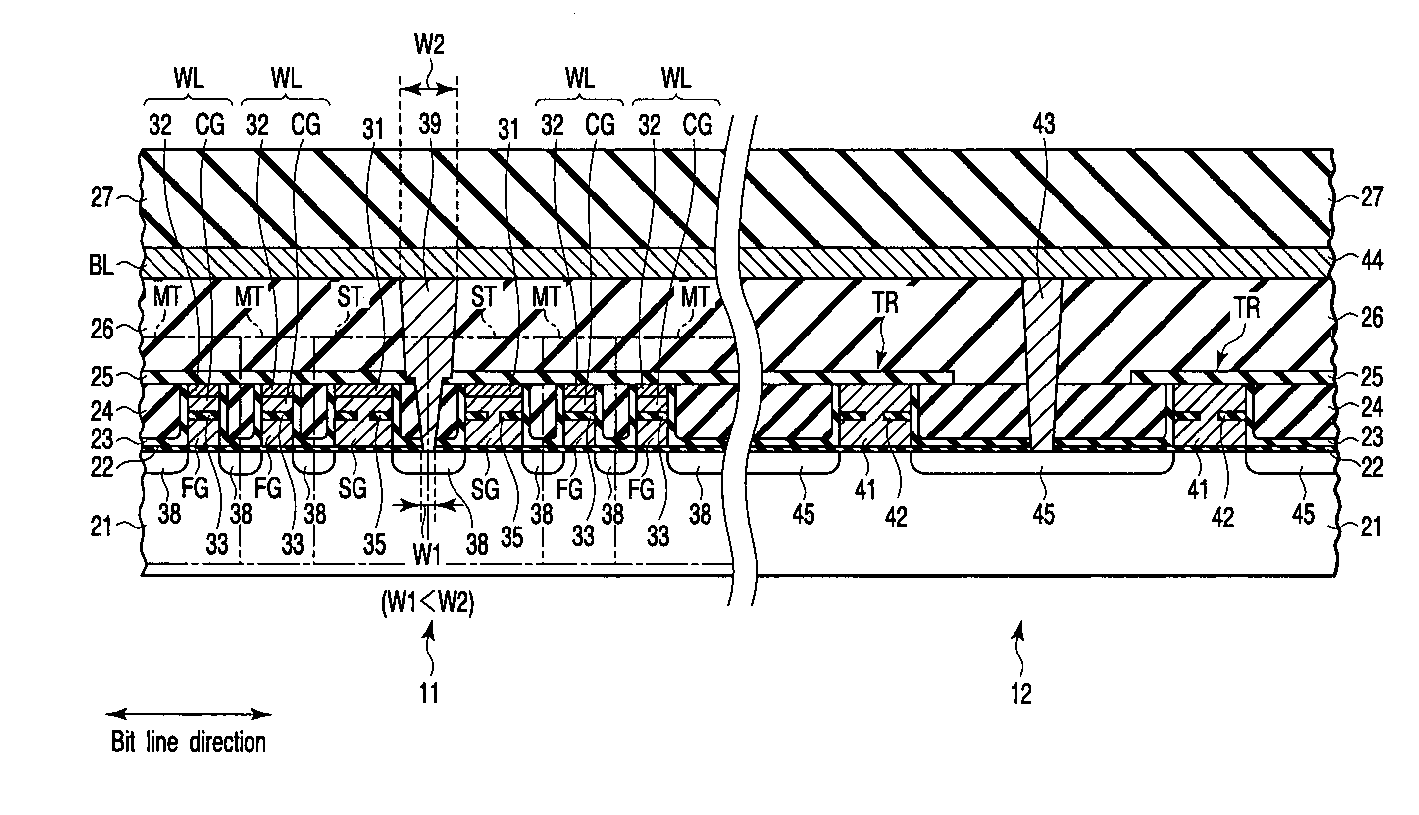
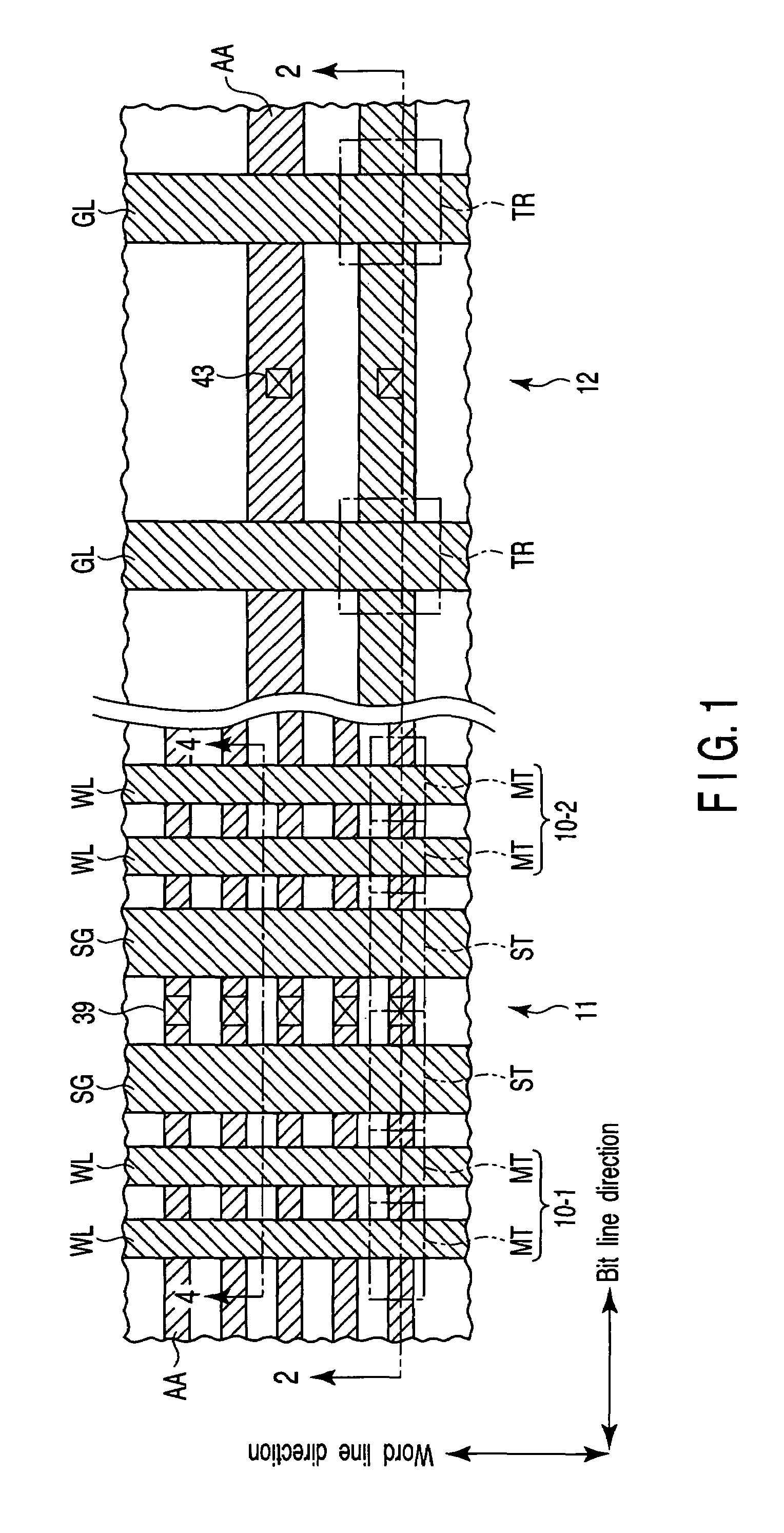
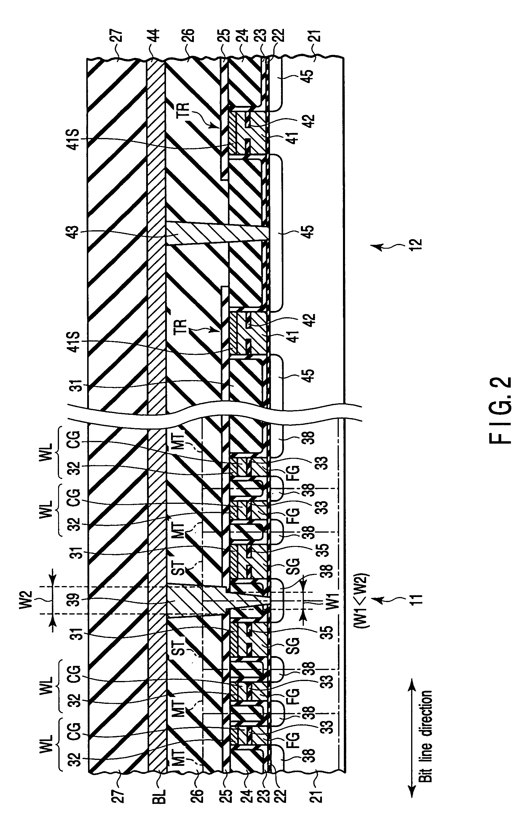
[0048]The structure of a semiconductor device according to a first embodiment of the invention is described referring to FIG. 1 to FIG. 4.

[0049]FIG. 1 is a plan view that schematically shows the semiconductor device according to the first embodiment. FIG. 2 is a cross-sectional structural view taken along line 2—2 in FIG. 1. FIG. 3 is a cross-sectional structural view that shows, in enlarged scale, a contact plug 39 near a barrier film 25 in FIG. 2. FIG. 4 is a cross-sectional structural view taken along line 4—4 in FIG. 1. In this embodiment, a NAND type flash memory is described by way of example.

[0050]As is shown in the Figures, a memory cell array 11 and a peripheral circuit 12 are provided on a major surface of a semiconductor (silicon) substrate 21.

[0051]The memory cell array 11 includes memory cell rows 10-1 and 10-2 that are arranged in a bit line direction, and select transistors ST. The select transistors ST select memory cell rows 10-1 and 10-2.

[0052]The memory cell row 1...

modification 1 (

[Modification 1 (Modification of Etching Mask)]

[0107]A method of manufacturing a semiconductor device according to Modification 1 of the present invention will now be described with reference to FIG. 15 and FIG. 16. Modification 1 relates to the photoresist 60 in the above-described first embodiment. FIG. 15 and FIG. 16 are plan views that schematically show a photoresist 60 for use in the manufacturing method of the semiconductor device according to Modification 1. A description of the parts common to those of the first embodiment is omitted.

[0108]A photoresist 60 shown in FIG. 15 has a trench 61 that is formed in the word line direction with a width W2 greater than the width W1. With this photoresist 60, a so-called common source line is formed, wherein the diffusion layers 38 of the select transistors ST arranged along the word line direction cab be set at an equal potential.

[0109]A photomask 60 shown in FIG. 16 has circular opening portions 61 each having a diameter W2 that is g...

modification 2 (

[Modification 2 (Modification of Peripheral Circuit)]

[0114]A method of manufacturing a semiconductor device according to Modification 2 of the present invention will now be described with reference to FIG. 17 through FIG. 19. FIG. 17 is a cross-sectional view that schematically shows the structure of a semiconductor device according to Modification 2. FIG. 18 and FIG. 19 are cross-sectional structural views that schematically illustrate fabrication steps of the semiconductor device according to Modification 2. Modification 2 relates to the gate line GL of the peripheral circuit 12 in the first embodiment. A description of the parts common to those in the first embodiment is omitted.

[0115]According to the semiconductor device of Modification 2, the same advantageous effects as with the first embodiment are obtained. In addition, as shown in the Figures, the gate line GL of the peripheral transistor TR of the peripheral circuit 12 is not provided with a silicide layer. Thus, the selec...


PUM


Abstract

A semiconductor device comprising a first insulation layer, a second insulation layer, a first barrier film, a second barrier film, a diffusion layer. The device further comprises an upper contact hole, a lower contact hole, and a contact plug. The upper contact hole penetrates the second insulation layer and has a bottom in the second barrier film. The bottom has a width greater than a trench made in the first insulation layer, as measured in a direction crossing the widthwise direction of the trench. The lower contact hole penetrates the first insulation layer and first barrier film, communicates with the first contact hole via the trench and is provided on the diffusion layer. The upper portion of the lower contact hole has the same width as the trench. The contact plug is provided in the upper contact hole and lower contact hole.

Description

CROSS-REFERENCE TO RELATED APPLICATIONS[0001]This application is based upon and claims the benefit of priority from the prior Japanese Patent Application No. 2004-282336, filed Sep. 28, 2004, the entire contents of which are incorporated herein by reference.BACKGROUND OF THE INVENTION[0002]1. Field of the Invention[0003]The present invention relates generally to a semiconductor device and a method of manufacturing the same, and is applied to, for example, a select transistor for selecting memory cell transistors having current paths connected in series in a NAND type flash memory.[0004]2. Description of the Related Art[0005]With ever increasing development in fine patterning of cells, there is a tendency that contacts for electrically connecting, e.g. diffusion layers of cells become still finer. Furthermore, with the progress of the generation of cells, it becomes difficult to carry out microfabrication of contacts by so-called lithography technology.[0006]Jpn. Pat. Appln. KOKAI Pu...

Claims


Application Information

Patent Timeline
Patent Type & Authority Patents(United States)
IPC IPC(8): H01L23/48H01L23/52H01L29/40
CPCH01L27/105H01L27/11529H01L27/11526H01L27/115H10B41/40H10B41/41H10B69/00H01L21/18H01L27/088H01L21/768
Inventor SAKUMA, MAKOTOMATSUNAGA, YASUHIKOARAI, FUMITAKASUGIMAE, KIKUKO
Owner KK TOSHIBA
Why Eureka
Try Eureka