Check patentability & draft patents in minutes with Patsnap Eureka AI!

Data processing apparatus

data processing technology, applied in the direction of program control, computation using denominational number representation, instruments, etc., can solve the problems of increasing circuitry scale, repeat instruction is not necessarily supported, and the control method used by digital signal processors such as those of prior art 1 and prior art 2 cannot be applied to a data processing apparatus provided with no repeat instruction, so as to reduce the power consumed for memory accessing

Inactive Publication Date: 2006-07-18
HITACHI LTD
View PDF22 Cites 4 Cited by
  • Summary
  • Abstract
  • Description
  • Claims
  • Application Information

AI Technical Summary

Benefits of technology

[0010]An object of the present invention is to provide a data processing apparatus provided with a control means which, in spite of the unavailability of a repeat instruction, reduces the power needed for memory accessing by reading instructions from a small scale buffer reiteratively during loop processing.
[0025]For instance, the data processing apparatus (100), in order to read out an instruction reiteratively from a buffer (104) in executing a loop, has only to insert an instruction to set a specific bit (124, a buffer control flag) immediately before the execution of the bit. Therefore, it can reduce the power consumed for memory accessing by reiteratively reading the instruction out of the small scale buffer (104) when processing the loop without using a repeat instruction.

Problems solved by technology

Accordingly there is a problem that the control method uses by digital signal processors such as those of Prior Art 1 and Prior Art 2 cannot be applied to a data processing apparatus provided with no repeat instruction.
In microprocessors of the like for general use instead of specializing in digital signal processing, a repeat instruction is not necessarily supported.
Since, moreover, a repeat control circuit needs many items of hardware such as a repeat start address register, a repeat end address register, a repeat count register, a comparator and a down counter, this is based on a way of thinking that increasing the circuitry scale by introducing such a repeat control circuit is not necessarily advantageous to a microprocessor.
However, as the digital signal processors of Prior Art 1 and Prior Art 2 are provided with no such means and, on every occasion of loop processing, control to reiteratively read out instructions out of the instruction buffer is effected, they involve the problem that correct program processing cannot be accomplished when they come across a loop of a structure to which control to reiteratively read out instructions from the instruction buffer cannot be applied.
However, there is the problem that, as the same small capacity memory is accessed even during non-loop processing, the hit ratio drops, making it impossible to increase the speed of program processing.

Method used


Image

  • Data processing apparatus
  • Data processing apparatus
  • Data processing apparatus

Examples


embodiment 1

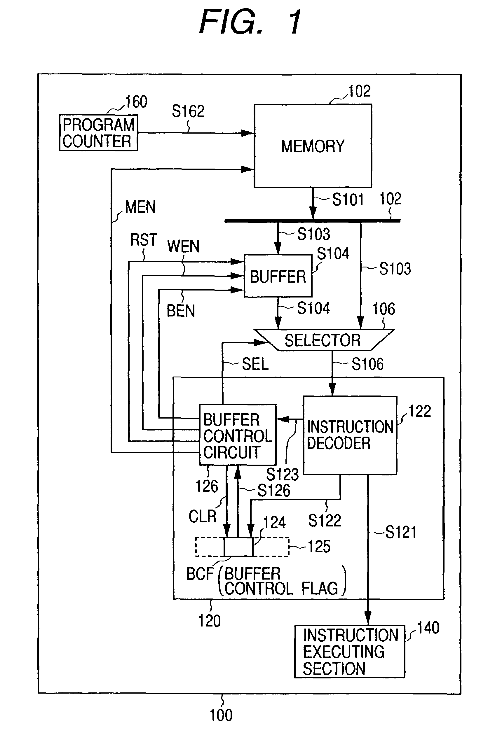
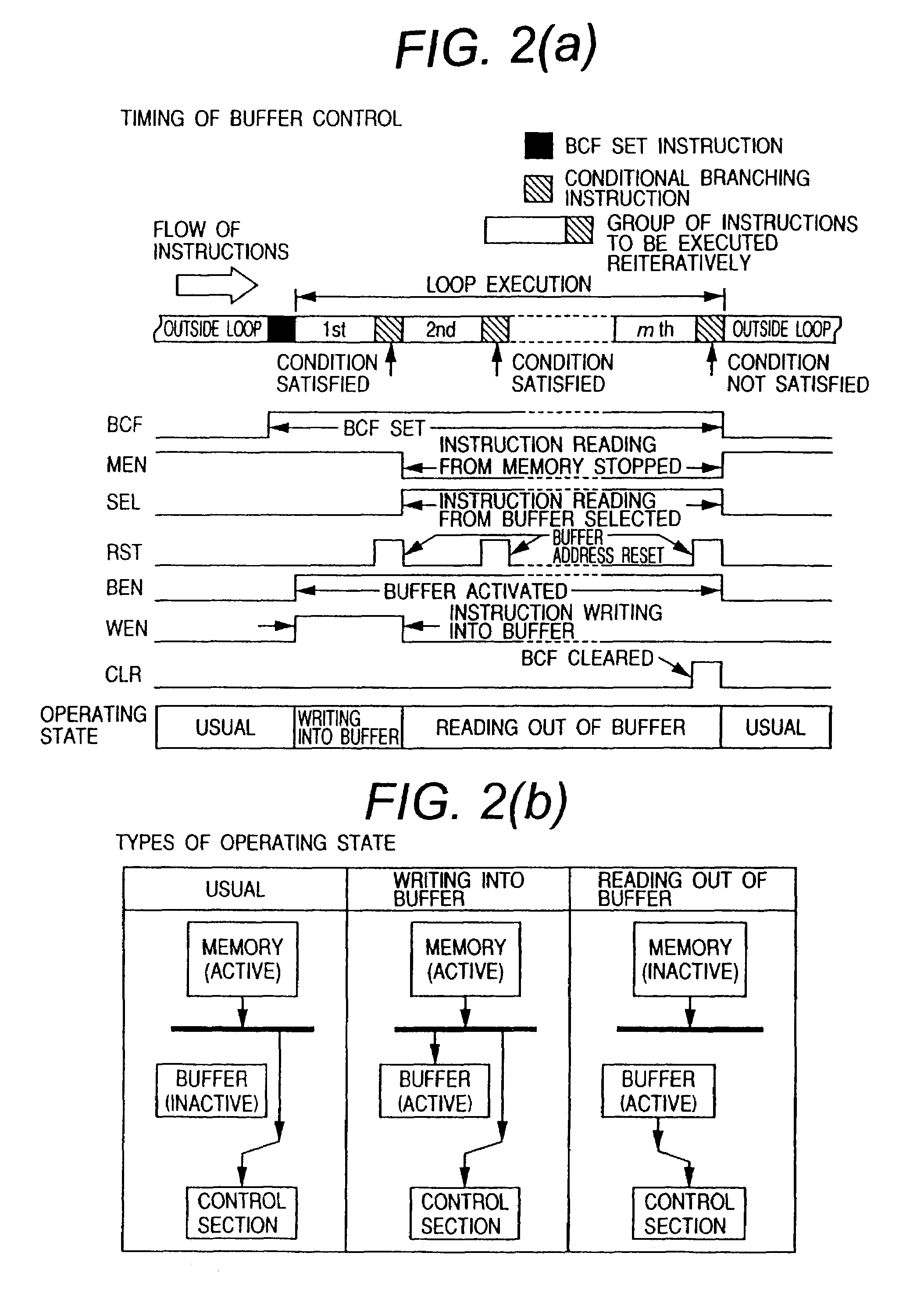
[0043]FIG. 1 illustrates the configuration of a data processing apparatus representing a first embodiment of the invention. A data processing apparatus 100 consists of a data processing section comprising a control section 120, an instruction executing section 140, a program counter 160, a buffer 104, a selector 106 and the like, and of a memory 102. The data processing apparatus 100 may either be formed over a single semiconductor substrate or only the aforementioned data processing section may be formed over a single semiconductor substrate. The control section 120 consists of an instruction decoder 122, a control register 125, a buffer control circuit 126 and the like. To add, instruction fetch queues(instruction pre-reading buffers) may as well be provided either within the instruction decoder 122 or between the selector 106 and the instruction decoder 122.

[0044]The memory 102 is, for example, either a read only memory (ROM) or random access memory (RAM) as a main storage or a c...

embodiment 2

[0107]FIG. 5 illustrates the configuration of a data processing apparatus representing a second embodiment of the present invention. A data processing apparatus 700 consists of a data processing section comprising a control section 720, an instruction executing section 740, a program counter 760, a buffer 704, a selector 706 and the like, and of a memory 702. The data processing apparatus 700 may either be formed over a single semiconductor substrate or only the aforementioned data processing section may be formed over a single semiconductor substrate. The control section 720 consists of an instruction decoder 722, a buffer control circuit 724 and the like. To add, instruction fetch queues (instruction pre-reading buffers) may as well be provided either within the instruction decoder722 or between the selector 706 and the instruction decoder 722.

[0108]The memory 702 is, for example, either a read only memory (ROM) or random access memory (RAM) as a main storage or a cache memory for...

embodiment 3

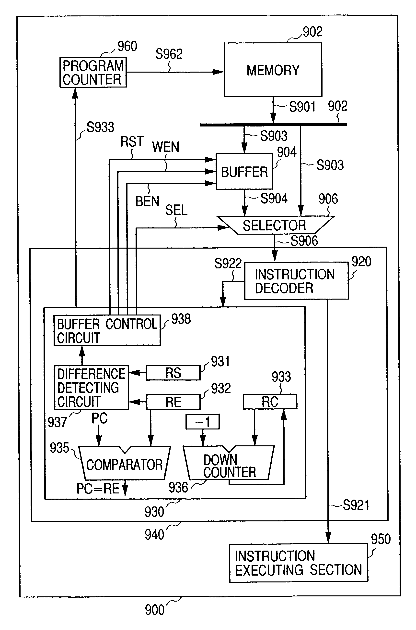
[0158]FIG. 7 illustrates the configuration of a data processing apparatus representing a third embodiment of the invention. A data processing apparatus 900 consists of a data processing section comprising a control section 940, an instruction executing section 950, a program counter 960, a buffer 904, a selector 906 and the like, and of a memory 902. The data processing apparatus 900 may either be formed over a single semiconductor substrate or only the aforementioned data processing section may be formed over a single semiconductor substrate. The control section 940 consists of an instruction decoder 920, a repeat control section 930 and the like. To add, instruction fetch queues (instruction pre-reading buffers) may as well be provided either within the instruction decoder 920 or between the selector 906 and the instruction decoder 920.

[0159]The memory 902 is, for example, either a read only memory (ROM) or random access memory (RAM) as a main storage or a cache memory for holding...


PUM


Abstract

A data processor apparatus having first and second instruction storages for holding a series of instructions to be executed reiteratively. The number of instructions is calculated based on the difference between a start address and an end address respectively stored in a start address register and an end address register. When the number of instructions constituting the series of instructions is less than the capacity of the second instruction storage, the series of instructions is read from the second instruction storage and executed. When the number of instructions is greater than the capacity of the second instruction storage, the series of instructions is read from the first instruction storage.

Description

[0001]This is a continuation application of U.S. Ser. No. 09 / 367,536, filed on Aug. 16, 1999 now U.S. Pat. No. 6,505,295.TECHNICAL FIELD[0002]The present invention relates to a data processing apparatus such as a microprocessor or a digital signal process (DSP), and more particularly to a technique effectively applicable to instruction buffers.BACKGROUND ART[0003]Along with the development of sophisticated information apparatuses including personal computers (PCs), personal digital assistants (PDAs), digital cellular units and car navigation aids in recent years, the need to reduce power consumption of large scale integrated circuits (LSIs) mounted on these apparatuses has tremendously increased. This is due to the requirements to make the batteries of portable information devices to keep their charged state longer and to suppress the costs of chip packages and cooling systems for desktop information devices. On the other hand, there are now increasingly active trends to incorporate...

Claims


Application Information

Patent Timeline
IPC IPC(8): G06F9/40G06F9/32G06F9/38
CPCG06F9/381G06F9/325
Inventor HIRAKI, MITSURUKIUCHI, ATSUSHIHAGIWARA, KESAMI
Owner HITACHI LTD
Features
  • R&D
  • Intellectual Property
  • Life Sciences
  • Materials
  • Tech Scout
  • Unparalleled Data Quality
  • Higher Quality Content
  • 60% Fewer Hallucinations
Learn More