Gate dielectric structure for reducing boron penetration and current leakage

Inactive Publication Date: 2006-07-25
BELL SEMICON LLC
View PDF14 Cites 4 Cited by
  • Summary
  • Abstract
  • Description
  • Claims
  • Application Information

AI Technical Summary

Benefits of technology

[0009]To address the above-discussed deficiencies of the prior art, the present invention provides a semiconductor device capable of substantially retarding boron penetration and reducing leakage current, within the semiconductor device, and a method of manufacture therefor. In the present invention the semiconductor device i

Problems solved by technology

As transistor channels shrink below 50 nm the limitations of conventional transistor processing, associated with such boron implants, has become more apparent.
However, as the gate oxide thickness has decreased, devices have become more susceptible to diffusion of boron dopants through the gate oxide and into the active area of the transistor.
The presence of these dopants within the channel region, can undesirably alter the threshold voltage of the device and may cause the device to be unstable due to threshold voltage drifting.
This problem is especially acute for boron implanted gate structures.
In addition to reliability concerns, thin gate oxides present significant manufacturing chall

Method used


Image

  • Gate dielectric structure for reducing boron penetration and current leakage
  • Gate dielectric structure for reducing boron penetration and current leakage
  • Gate dielectric structure for reducing boron penetration and current leakage

Examples


Embodiment Construction

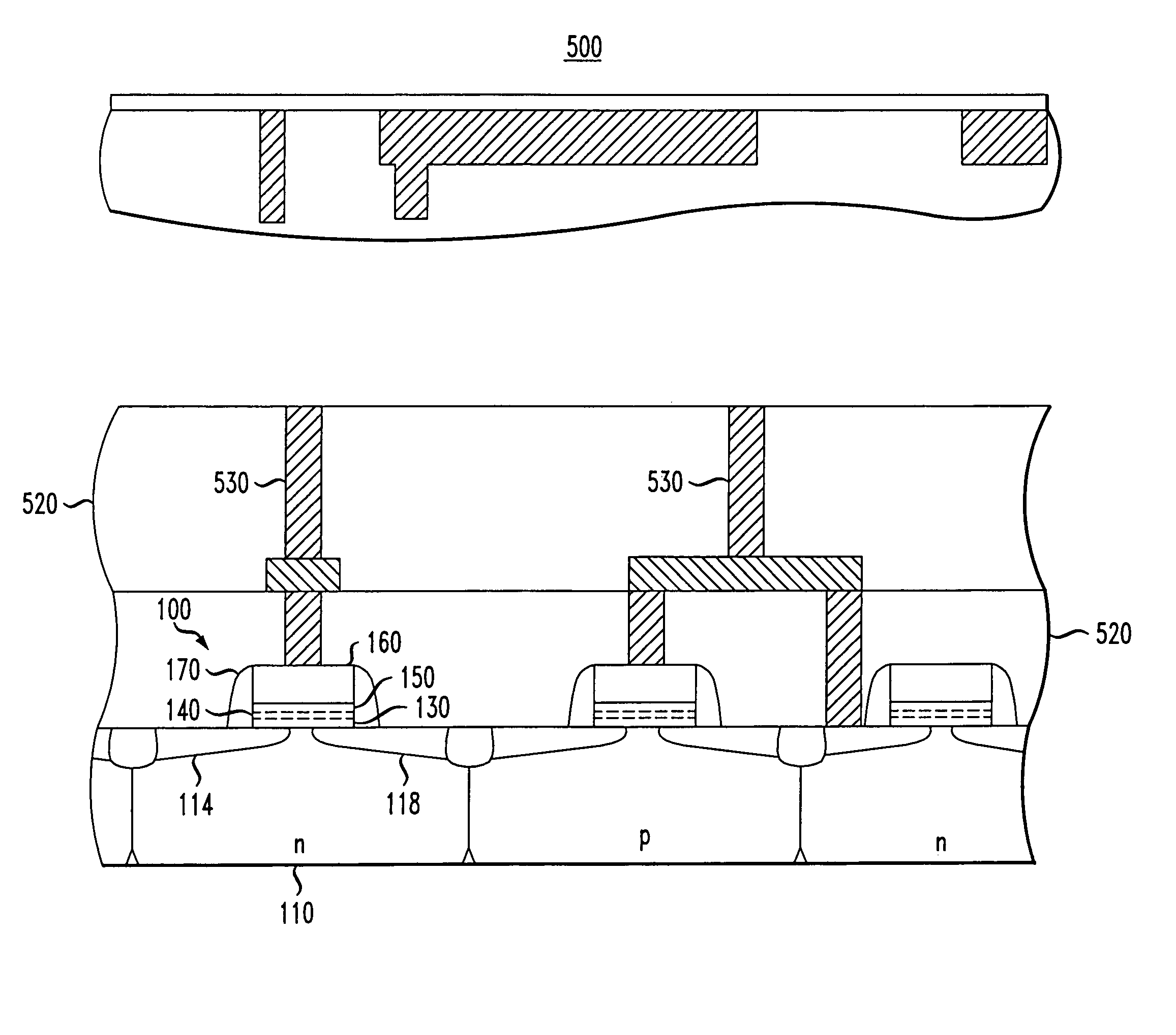
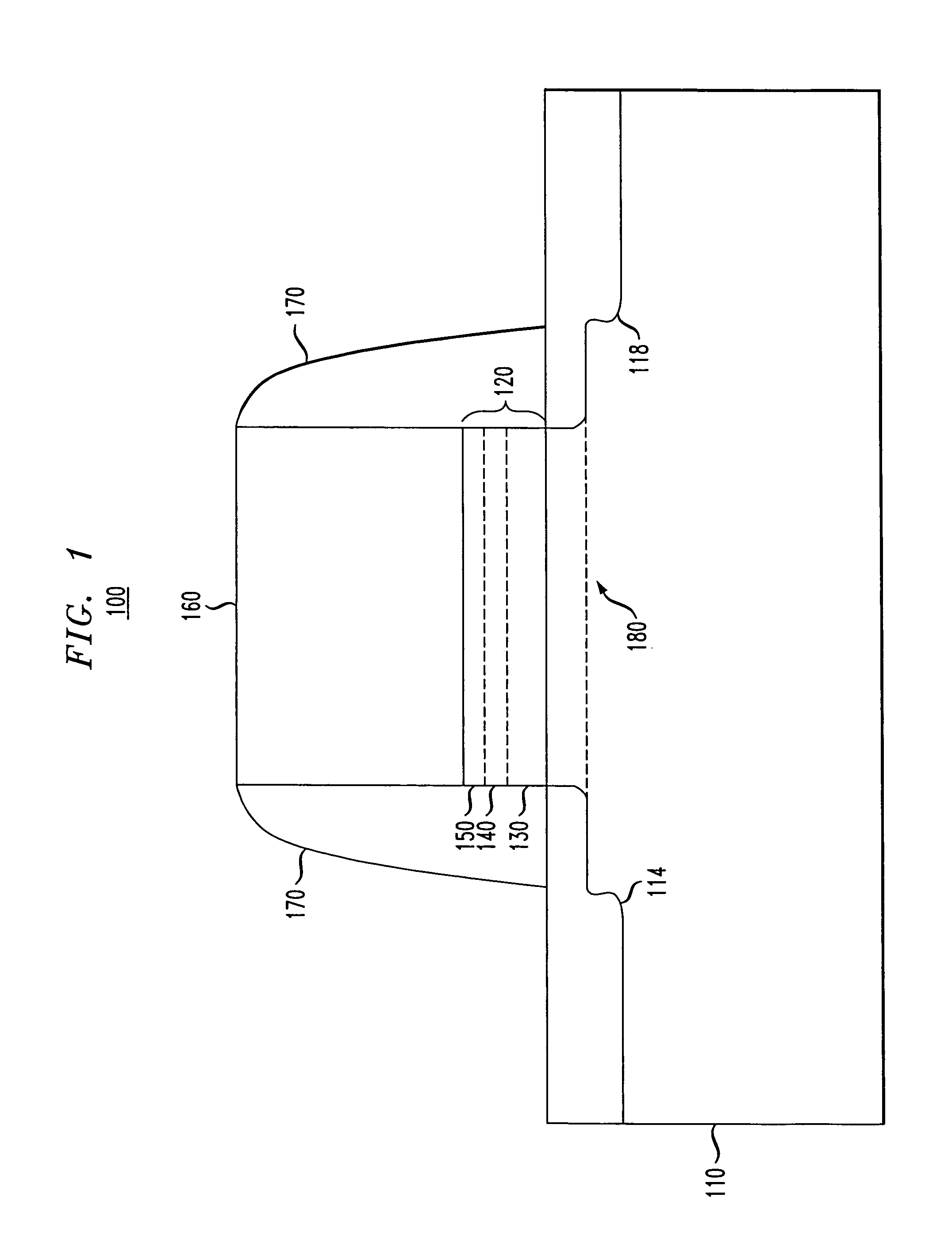
[0020]Referring initially to FIG. 1, illustrated is a cross-sectional view of a completed semiconductor device 100 manufactured by the method described herein. The semiconductor device 100 includes a semiconductor wafer substrate 110, a source region 114 and a drain region 118. It should be noted that the semiconductor wafer substrate 110 may be any layer located in the semiconductor device 100. Also included in the semiconductor device 100 is a gate dielectric 120 located over the semiconductor wafer substrate 110. The gate dielectric 120 includes a dielectric layer 130 and a nitrided layer 150, with a nitrided transition region 140 located therebetween. Typically the dielectric layer 130 and the nitrided layer 150 have thicknesses ranging from about 0.5 nm to about 2.0 nm and from about 0.25 nm to about 1.0 nm, respectively. Also included in the semiconductor device 100 is a gate 160 located over the gate dielectric 120, and oxide spacers 170.

[0021]The semiconductor device 100 man...


PUM


Abstract

The present invention provides a semiconductor device capable of substantially retarding boron penetration within the semiconductor device and a method of manufacture therefor. In the present invention the semiconductor device includes a gate dielectric located over a substrate of a semiconductor wafer, wherein the gate dielectric includes a nitrided layer and a dielectric layer. The present invention further includes a nitrided transition region located between the dielectric layer and the nitrided layer and a gate located over the gate dielectric.

Description

[0001]This Application is a Divisional of prior application Ser. No. 09 / 605,931 entitled “A NOVEL GATE DIELECTRIC STRUCTURE FOR REDUCING BORON PENETRATION AND CURRENT LEAKAGE,” to Yuan Chen, et al., filed on Jun. 28, 2000 now abandoned. The above-listed Application is commonly assigned with the present invention and is incorporated herein by reference as if reproduced herein in its entirety under Rule 1.53(b).TECHNICAL FIELD OF THE INVENTION[0002]The present invention is directed, in general, to a semiconductor device and, more specifically, to a semiconductor device having a nitrided transition region located between a dielectric layer and a nitrided layer, that substantially retards boron penetration and current leakage, and a method of manufacture therefor.BACKGROUND OF THE INVENTION[0003]The fabrication of metal-oxide-semiconductor (MOS) transistors within a semiconductor substrate is well known. These MOS transistors include a plurality of polysilicon gate structures that are f...

Claims


Application Information

Patent Timeline
IPC IPC(8): H01L21/31H01L21/28H01L29/51H01L29/76
CPCH01L21/28202H01L29/513
Inventor CHEN, YUANLI, FENGMA, YISTEINER, KURT G.
Owner BELL SEMICON LLC
Why Eureka
Try Eureka