Treatment for corrosion in substrate processing

a substrate processing and corrosion technology, applied in the direction of cleaning processes and utensils, chemistry apparatus and processes, electrical utensils, etc., can solve the problem of failing to teach a selective etching method of silicon carbide (sic) at an etch ra

Inactive Publication Date: 2006-08-01
LAM RES CORP
View PDF57 Cites 238 Cited by
  • Summary
  • Abstract
  • Description
  • Claims
  • Application Information

AI Technical Summary

Problems solved by technology

However, each of these patents fail to teach a method for selectively etching silic...

Method used


Image

  • Treatment for corrosion in substrate processing
  • Treatment for corrosion in substrate processing
  • Treatment for corrosion in substrate processing

Examples


Embodiment Construction

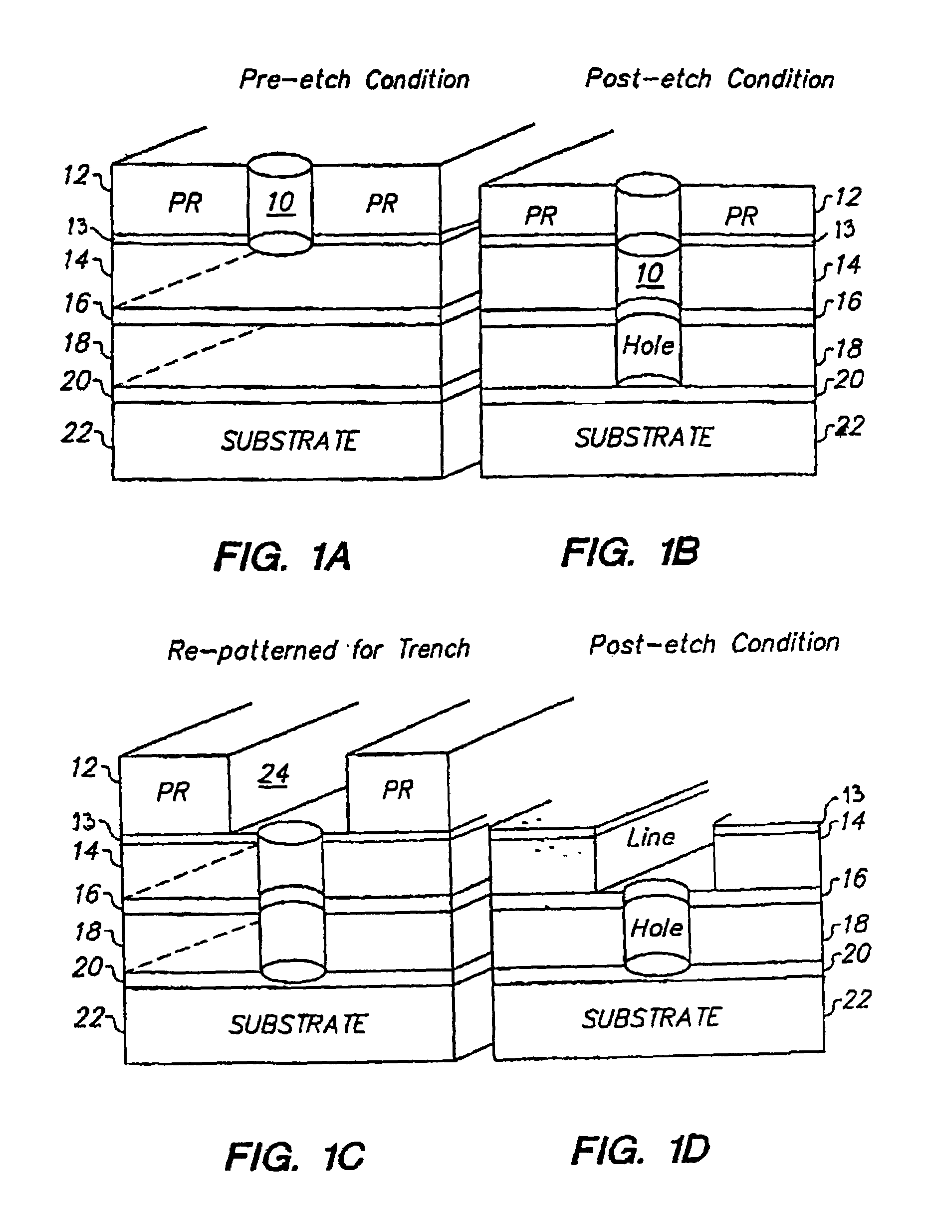
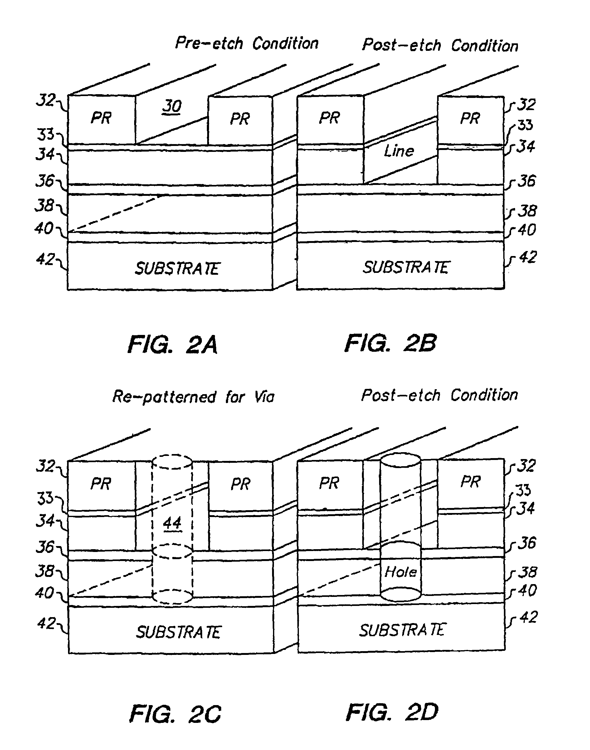
[0020]In the following detailed description, reference is made to the accompanying drawings, which form a part of this application. The drawings show, by way of illustration, specific embodiments in which the invention may be practiced. It is to be understood that other embodiments may be utilized and structural changes may be made without departing from the scope of the present invention.

[0021]The invention provides a process for plasma etching silicon carbide (SiC) with selectivity to an overlapping an / or underlying dielectric layer of material. The dielectric material can comprise various low-k dielectric materials, including organic low-k materials, inorganic dielectric materials, silicon dioxide, silicon oxynitride, or the like. In order to achieve a desired selectivity to such dielectric materials, the plasma etch gas chemistry is selected to achieve a desired etch rate of the silicon carbide while etching the dielectric material at a slower rate.

[0022]Silicon carbide has favo...


PUM

PropertyMeasurementUnit
Fractionaaaaaaaaaa
Fractionaaaaaaaaaa
Percent by volumeaaaaaaaaaa

Abstract

A method for processing substrate to form a semiconductor device is disclosed. The substrate includes an etch stop layer disposed above a metal layer. The method includes etching through the etch stop layer down to the copper metal layer, using a plasma etch process that utilizes a chlorine-containing etchant source gas, thereby forming etch stop layer openings in the etch stop layer. The etch stop layer includes at least one of a SiN and SiC material. Thereafter, the method includes performing a wet treatment on the substrate using a solution that contains acetic acid (CH3COOH) or acetic acid/ammonium hydroxide (NH4OH) to remove at least some of the copper oxides. Alternatively, the copper oxides may be removed using a H2 plasma. BTA passivation may be optionally performed on the substrate.

Description

CROSS REFERENCE[0001]This patent application is a continuation in part of patent application Ser. No. 10 / 199,190, entitled “A method for Etching Silicon Carbide”, which was filed on Jul. 19, 2002, now U.S. Pat. No. 6,919,278, which is a continuation in part of application Ser. No. 09 / 820,696 entitled “plasma Etching of Silicon Carbide” which was filed on Mar. 30, 2001, now abandoned, all of which are incorporated by reference herein.BACKGROUND OF THE INVENTION[0002]The present invention relates to the etching of dielectric materials. More particularly, the present invention is related to the selective etching of silicon carbide using a chlorine containing gas.[0003]The manufacture of multilayer structures typically involves patterned etching of areas of the semiconductor surface that are covered by a photoresist protective material. One etching technique is reactive ion etching (RIE). This process involves positioning a semiconductor wafer in a reaction chamber and feeding etchant g...

Claims


Application Information

Patent Timeline
IPC IPC(8): H01L21/461H01L21/302
CPCH01L21/31111H01L21/31116H01L21/32137H01L21/76814H01L21/76802H01L21/76807H01L21/7681H01L21/32138
Inventor LEE, SANGHEONKANG, SEAN S.SADJADI, S M REZADESHMUKH, SUBHASHKIM, JI SOO
Owner LAM RES CORP
Why Eureka
Try Eureka