Impedance adjustment circuit, impedance adjustment method, and semiconductor device

a technology of impedance adjustment and semiconductor devices, applied in the field of semiconductor integrated circuits, can solve problems such as noise increase, input buffer error invitation, performance degradation, etc., and achieve the effect of preventing noise-induced errors

Inactive Publication Date: 2006-08-01
NEC CORP
View PDF20 Cites 17 Cited by
  • Summary
  • Abstract
  • Description
  • Claims
  • Application Information

AI Technical Summary

Benefits of technology

[0021]The present invention was made in view of these conventional problems, and an object of the present invention is to provide an impedance adjustment circuit capable of preventing errors caused by noises.

Problems solved by technology

The reason is that mismatch between the impedance of a transmission line and the impedance of a load causes a reflected wave, which then invites errors of an input buffer.
However, if the size of the MOS transistor is enlarged, the LSI will cause a problem that its performance is deteriorated, because of deterioration of mountability inside the LSI, increase in penetrating currents, increase in noises, increase in the amount of electricity consumed, etc.
However, since an impedance adjustment circuit is placed inside an LSI, it might cause errors due to noises (power source noises, etc.) caused by itself or noises received from surrounding circuits.
However, since a noise in an LSI has around several ten mV, errors will be caused if a noise is mixed into a detection signal from the comparator.

Method used


Image

  • Impedance adjustment circuit, impedance adjustment method, and semiconductor device
  • Impedance adjustment circuit, impedance adjustment method, and semiconductor device
  • Impedance adjustment circuit, impedance adjustment method, and semiconductor device

Examples


Embodiment Construction

[0040]An impedance adjustment circuit according to an embodiment of the present invention will now be explained with reference to the drawings.

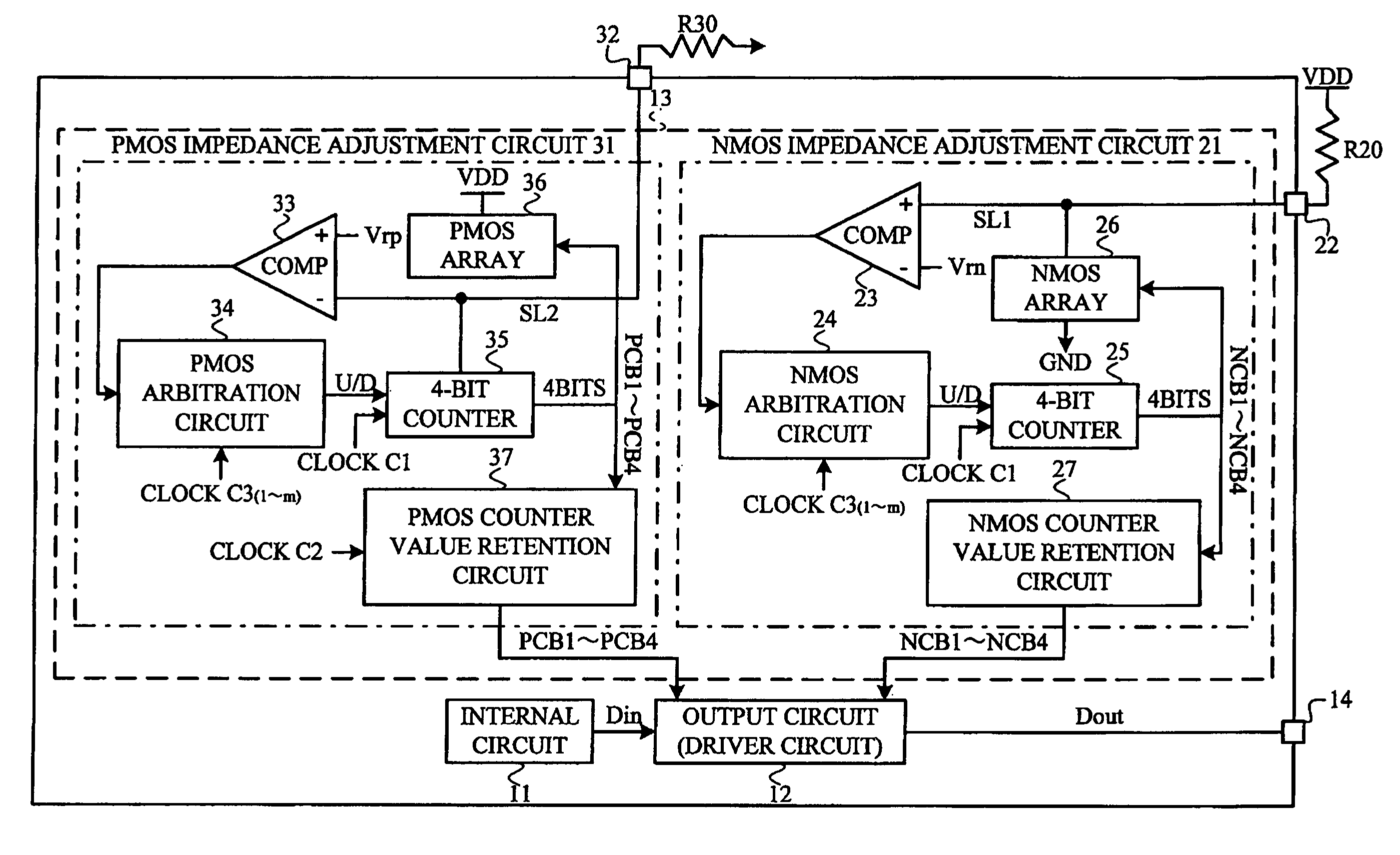
[0041]First, the entire configuration of a semiconductor integrated circuit including an impedance adjustment circuit will be explained with reference to a circuitry diagram shown in FIG. 1.

[0042]As shown in FIG. 1, a semiconductor device (hereinafter referred to as LSI) 10 comprises an internal circuit 11, an output circuit 12, and an impedance adjustment circuit 13.

[0043]The internal circuit 11 performs various signal processes and outputs a signal Din to be output outside the LSI 10. The signal Din is a binary signal having a high level and a low level.

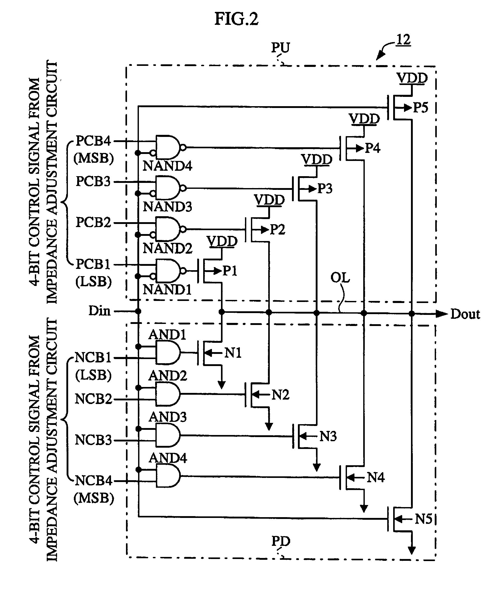
[0044]The output circuit 12 expands the dynamic range and current-driving capability of the signal Din output from the internal circuit 11, and outputs the expanded signal as a signal Dout. The signal Dout is output to the outside via an output terminal 14 of the LSI 10.

[0045]The impedance a...


PUM


Abstract

An impedance adjustment circuit has an external resistor, a comparator which compares the potential of one terminal of the external resistor with a predetermined voltage, a counter whose counted value changes in accordance with an output from the comparator and which outputs a control signal corresponding to the counted value, an NMOS array whose value of resistance changes in accordance with the control signal and which is connected to one terminal of the external resistor and an NMOS arbitration circuit which detects an output from the NMOS comparator a plurality of times and outputs a signal determined by a majority decision logic taken on the detected signals to the counter.

Description

BACKGROUND OF THE INVENTION[0001]1. Field of the Invention[0002]The present invention relates to a semiconductor integrated circuit, and particularly, to an impedance adjustment circuit which can adjust output impedance, input impedance, etc., an impedance adjustment method, and a semiconductor device comprising this impedance adjustment circuit.[0003]2. Description of the Related Art[0004]A high-speed interface is required to function as a sending circuit, a receiving circuit, a transmission line between LSIs, and a distributed constant circuit, and at the same time impedance matching is indispensable for a high-speed interface. The reason is that mismatch between the impedance of a transmission line and the impedance of a load causes a reflected wave, which then invites errors of an input buffer.[0005]Accordingly, a conventional output buffer circuit which performs a high-speed interface function has a built-in resistor at the output side thereof inside an LSI, or has a resistor c...

Claims


Application Information

Patent Timeline
Patent Type & Authority Patents(United States)
IPC IPC(8): H03K17/16H01L21/822G06F3/00H01L27/04H03K19/00H03K19/0175H03K19/23H04L25/02
CPCH03K19/0005H04L25/0278H04L25/028
Inventor OGURI, TAKASHI
Owner NEC CORP
Why Eureka
Try Eureka