Thin film magnetic head having spiral coils and manufacturing method thereof
a spiral coil and magnetic head technology, applied in the direction of heads with metal sheet cores, data recording, instruments, etc., can solve the problems of reducing the floating height of the slider, and reducing the resistance of the coil. , to achieve the effect of reducing the quantity of generated heat and lowering the resistance of the coil
- Summary
- Abstract
- Description
- Claims
- Application Information
AI Technical Summary
Benefits of technology
Problems solved by technology
Method used
Image

Examples
embodiment 1
(1) Embodiment 1
[0211]Embodiment 1 relating to a manufacturing method is a method for manufacturing the thin film magnetic head shown in FIGS. 1 to 5. It is notified in advance that processes illustrated in FIGS. 8 to 47 are performed on a wafer.
Process Leading to a State of FIG. 8
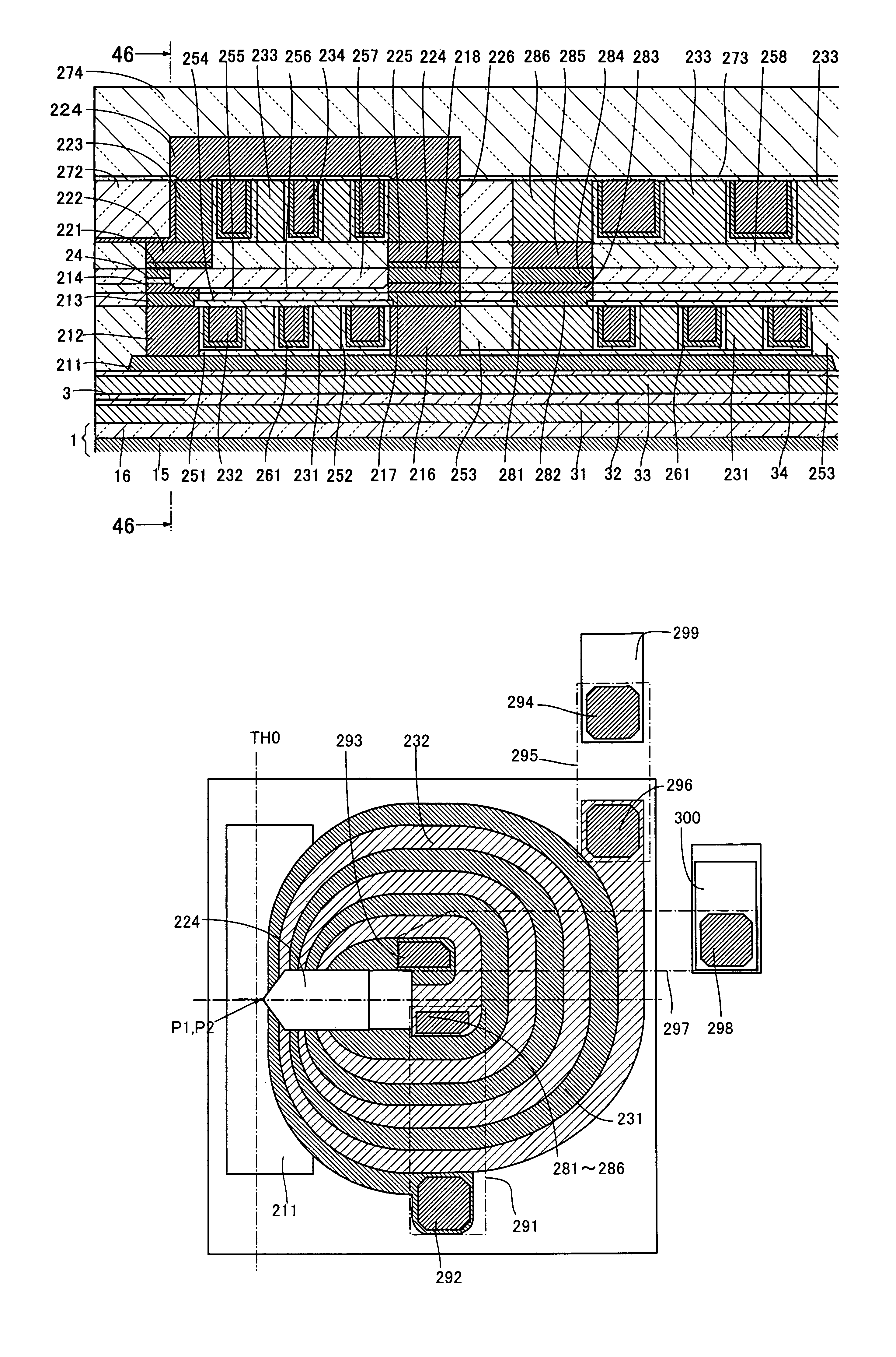
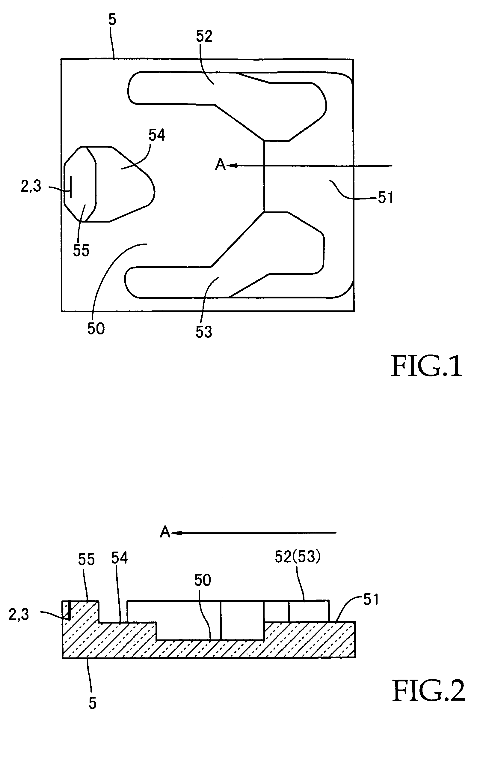
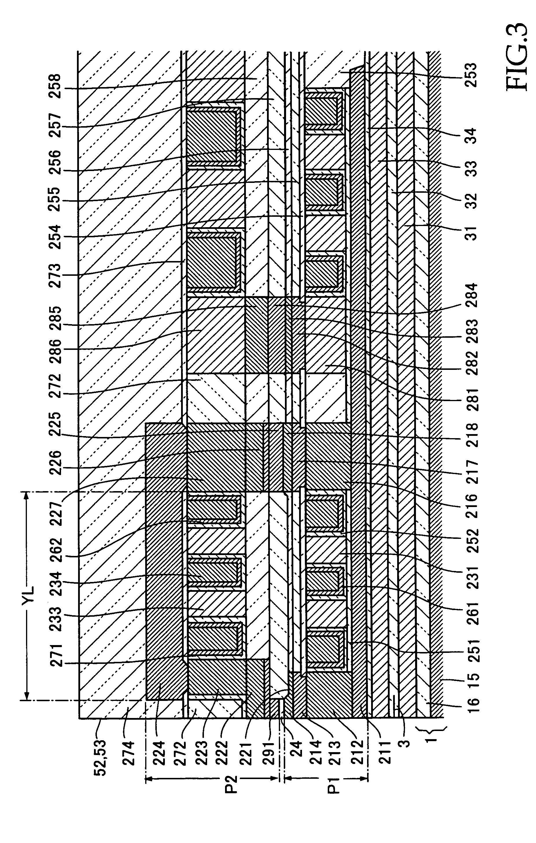
[0212]Referring to FIG. 8, on an insulating film 16 deposited on a base body 15 there are formed a first shield film 31, a read element 3, an insulating film 32, a second shield film 33, an insulating film 34 and a lower yoke 211 by means of publicly known processes. In one example, an insulating film 16, which is made of alumina or the like, is deposited about 3 μm in thickness on the base body 15. Next, to form the first shield film 31, a plating method is performed, using a photoresist film as a mask, to selectively deposit permalloy about 2 to 3 μm in thickness on the insulating film 16. Next, an alumina film (not illustrated) of about 3 to 4 μm in thickness is formed thereon and then is flattened by m...
embodiment 2
(2) Embodiment 2
[0265]Embodiment 2 is a method for manufacturing a thin film magnetic head shown in FIGS. 6 and 7, and is illustrated in FIGS. 48 to 79. It is notified in advance that processes illustrated in FIGS. 48 to 79 are also performed on a wafer.
Processes Leading to States of FIGS. 48 to 50
[0266]The processes leading to states of FIGS. 48 to 50 are substantially the same as the processes shown in FIGS. 8 to 10 in embodiment 1, and detailed description is omitted.
Process Leading to a State of FIG. 51
[0267]A photolithography process is applied onto a photoresist film RS2 in FIG. 50, and then IBE is performed so as to pattern a lower yoke 211 into a prescribed pattern. After that, the photoresist film RS2 is removed.
[0268]Next, an insulating film 252 is deposited on the surfaces and side surfaces of an insulating film 251, a first coil 231, a second lower pole film 212, a first back gap film 216 and a first connecting conductor film 281. The insulating film 252 is, specifically...
PUM
| Property | Measurement | Unit |
|---|---|---|
| frequency | aaaaa | aaaaa |
| height | aaaaa | aaaaa |
| height | aaaaa | aaaaa |
Abstract
Description
Claims
Application Information
 - R&D
- Intellectual Property
- Life Sciences
- Materials
- Tech Scout
- Unparalleled Data Quality
- Higher Quality Content
- 60% Fewer Hallucinations
Browse by: Latest US Patents, China's latest patents, Technical Efficacy Thesaurus, Application Domain, Technology Topic, Popular Technical Reports.
© 2025 PatSnap. All rights reserved.Legal|Privacy policy|Modern Slavery Act Transparency Statement|Sitemap|About US| Contact US: help@patsnap.com