
Word line driver circuit for a static random access memory and method therefor

a random access memory and driver circuit technology, applied in static storage, digital storage, instruments, etc., can solve the problems of static noise margin of a cell decreasing, logic state that is stored in the cell may be inadvertently changed,

Active Publication Date: 2006-08-01
NXP USA INC
View PDF5 Cites 47 Cited by
  • Summary
  • Abstract
  • Description
  • Claims
  • Application Information

AI Technical Summary

Benefits of technology

The present invention provides a method for improving the performance of a static random access memory (SRAM) by reducing the power supply voltage to the word line driver circuits while maintaining adequate static noise margin. By doing so, the SRAM can operate at lower voltages with adequate static noise margin. The invention also includes a data processing system that includes the SRAM and a word line driver power supply control circuit. The word line driver circuit includes a P-channel pull-up transistor and an N-channel pull-down transistor. The invention allows for improved performance of the SRAM in low power mode and reduces the likelihood of read disturb, which is a common problem in SRAMs.

Problems solved by technology

However, the static noise margin of a cell decreases as the power supply voltage decreases.
If the cell has inadequate noise margins, the logic state that is stored in the cell may be inadvertently changed when the cell is accessed for a read operation.

Method used


Image

  • Word line driver circuit for a static random access memory and method therefor
  • Word line driver circuit for a static random access memory and method therefor

Examples


Embodiment Construction

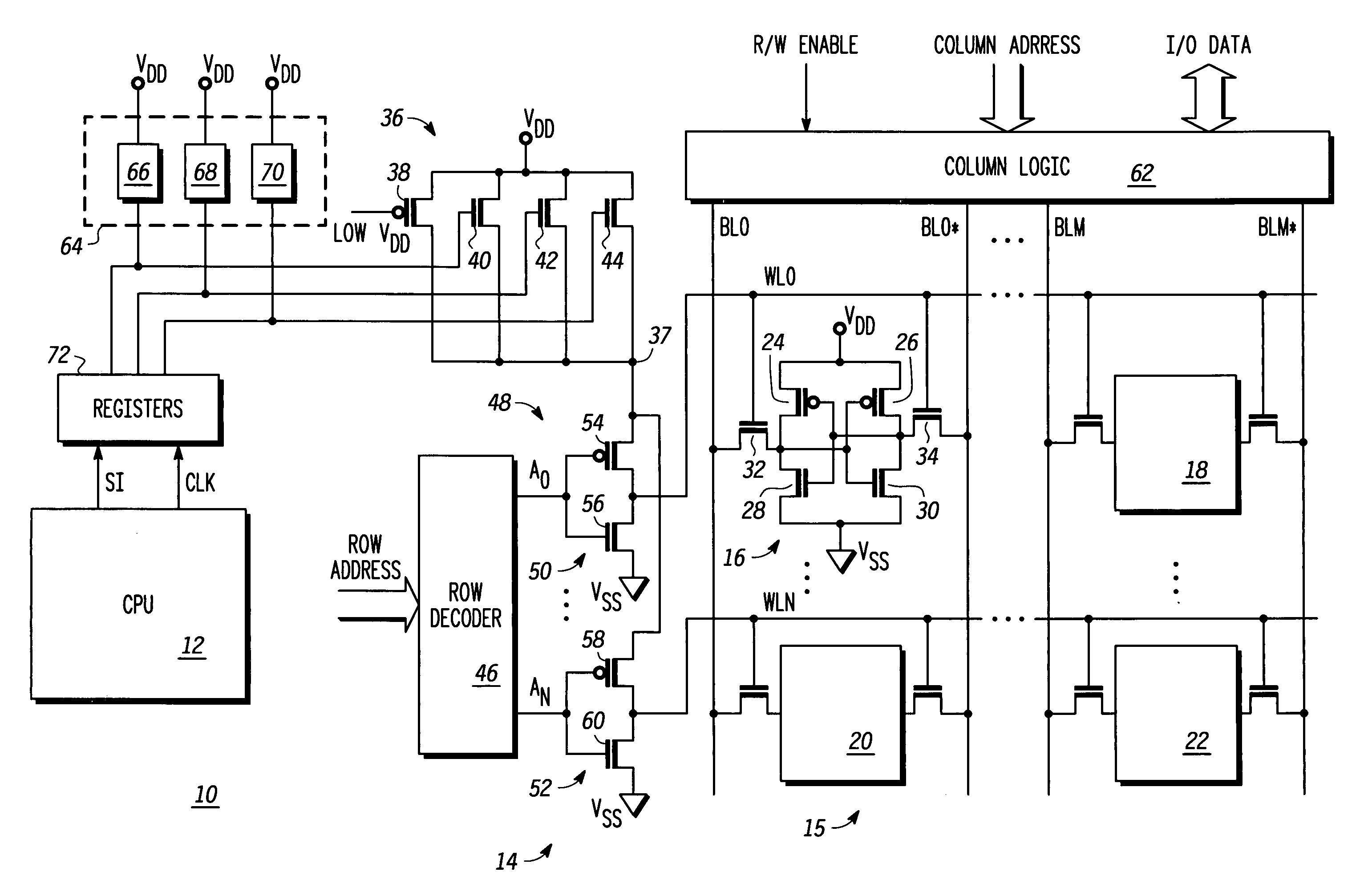
[0006]Generally, the present invention provides a data processing system having an embedded SRAM. During a low power mode of operation, the power supply voltage provided to the word line driver circuits of the memory is reduced by a predetermined voltage below the power supply voltage that is provided to the memory cells. By decreasing the word line driver voltage below the power supply voltage, the static noise margin of the memory array is improved for low voltage operation.

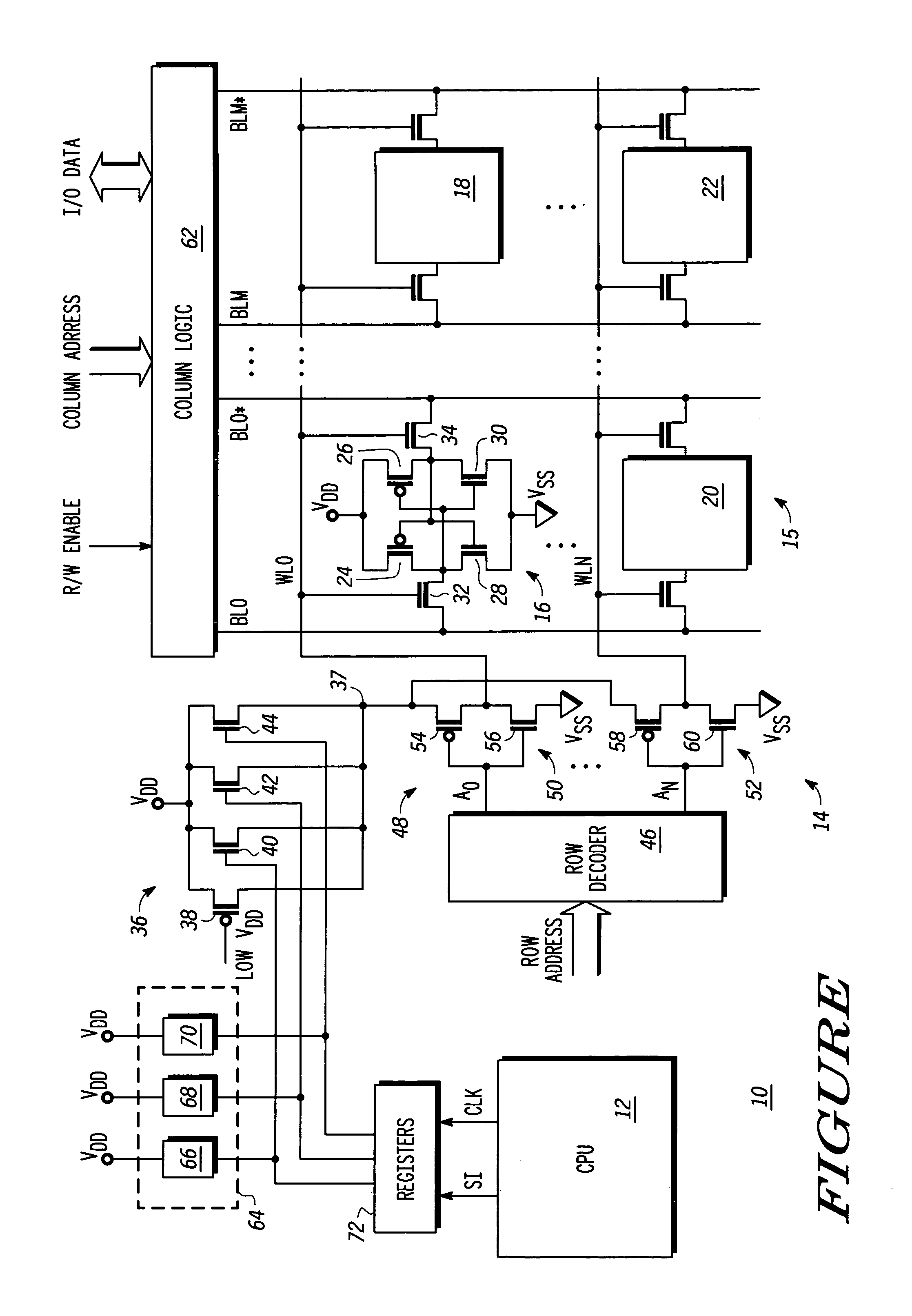
[0007]The FIGURE illustrates, in partial schematic diagram form and partial block diagram form, a data processing system 10 in accordance with the present invention. Data processing system 10 includes a central processing unit (CPU) 12, a memory 14, a word line driver power supply control circuit 36, fuse block circuit 64, and registers 72. The memory 14 includes a memory array 15, a row decoder 46, word line driver circuits 48, and column logic 62. The memory array 15 has representative SRAM cells 16, 18, 20, ...


PUM


Abstract

A static random access memory (14) has a normal mode of operation and a low voltage mode of operation. A memory array (15) includes memory cells (16) coupled to a first power supply node (VDD) for receiving a power supply voltage. A plurality of word line drivers is coupled to word lines of the memory array (15) and to a second power supply node (37). A word line driver voltage reduction circuit (36) has an input coupled to the first power supply node (VDD) and an output coupled to the second power supply node (37) for reducing a voltage on the output in relation to a voltage on the input in response to a low power supply voltage signal, and thus improving a static noise margin of the memory cells (16).

Description

FIELD OF THE INVENTION[0001]This invention relates generally to data processing systems and more particularly to a word line driver circuit for a static random access memory (SRAM) and method therefor.BACKGROUND OF THE INVENTION[0002]Static random access memories (SRAMs) are generally used in applications requiring high speed, such as a cache memory in a data processing system. A SRAM is usually implemented as an array of memory cells organized in rows and columns. Each SRAM cell stores one bit of data and is implemented as a pair of inverters having their inputs and outputs cross-coupled at differential storage nodes. The SRAM cell is “bistable”, that is, it is stable at one of two possible logic levels. The logic state of the cell is determined by whichever of the two inverter outputs is a logic high, and can be made to change states by applying a voltage of sufficient magnitude and duration to the appropriate cell input.[0003]Many applications for embedded SRAMs today require the...

Claims


Application Information

Patent Timeline
Patent Type & Authority Patents(United States)
IPC IPC(8): G11C7/00G11C11/00
CPCG11C11/413G11C8/08
Inventor REMINGTON, SCOTT I.BURNETT, JAMES D.
Owner NXP USA INC
Learn More