

Doping profiles in PN diode optical modulators
a technology of optical modulators and diodes, applied in the field of optical modulators, can solve the problems of low speed devices not being suitable for high speed ghz rate systems
- Summary
- Abstract
- Description
- Claims
- Application Information
AI Technical Summary
Benefits of technology
Problems solved by technology
Method used
Image

Examples
Embodiment Construction
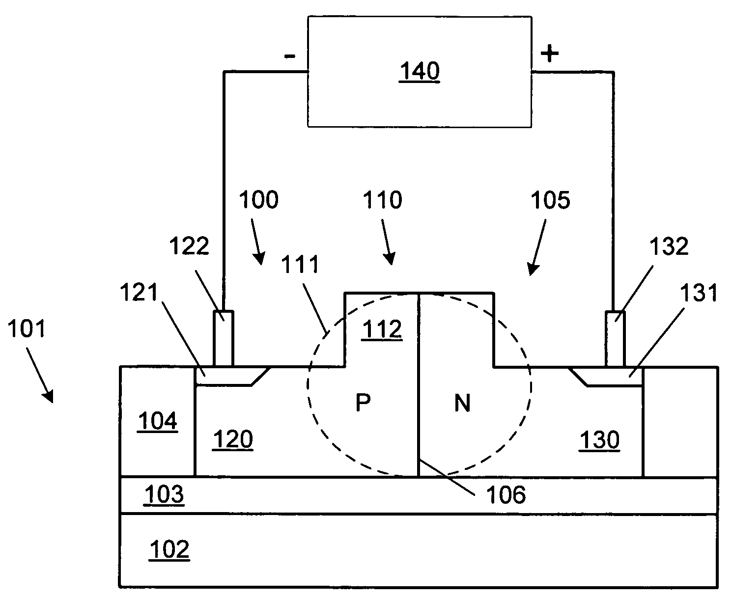
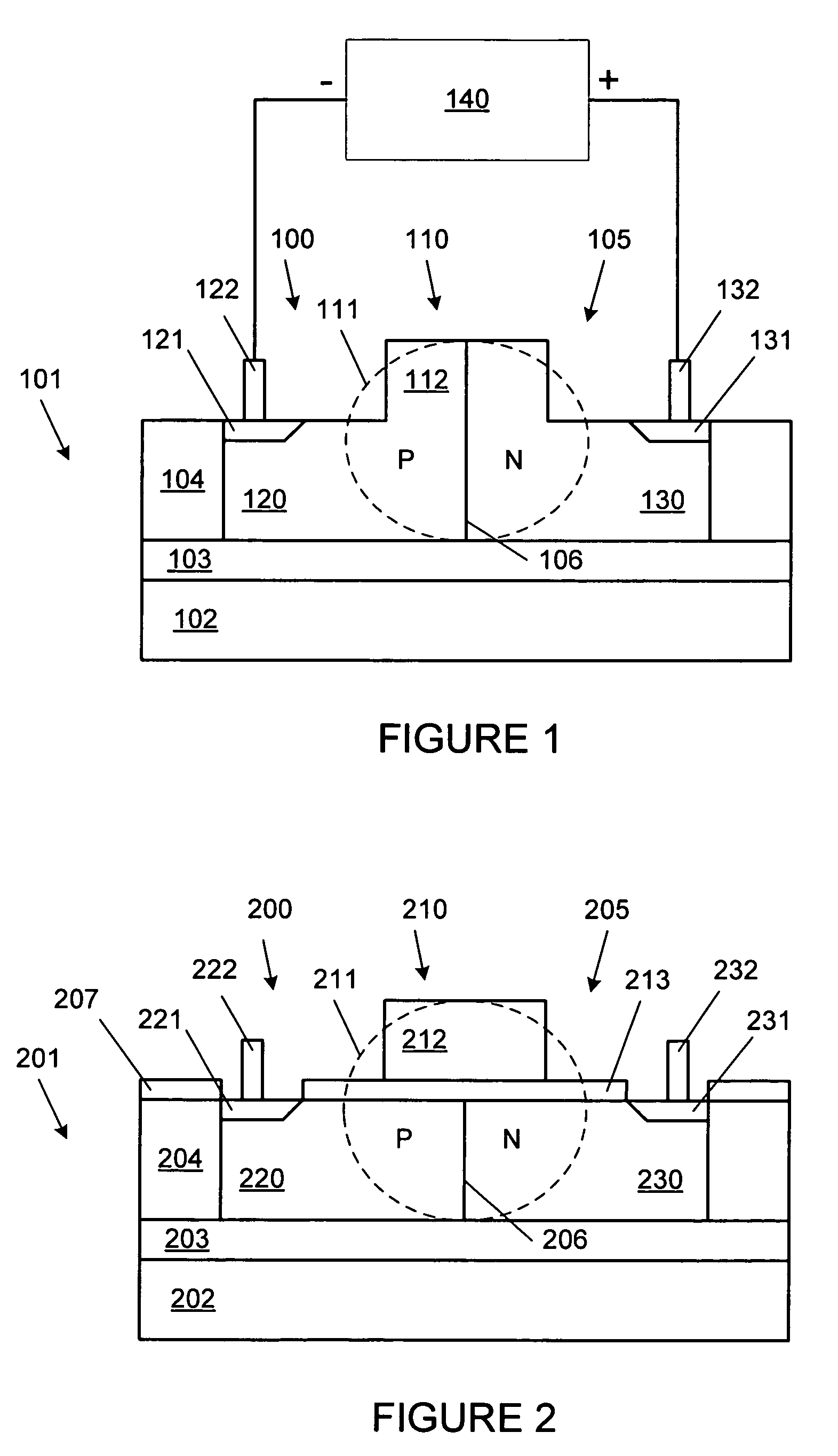
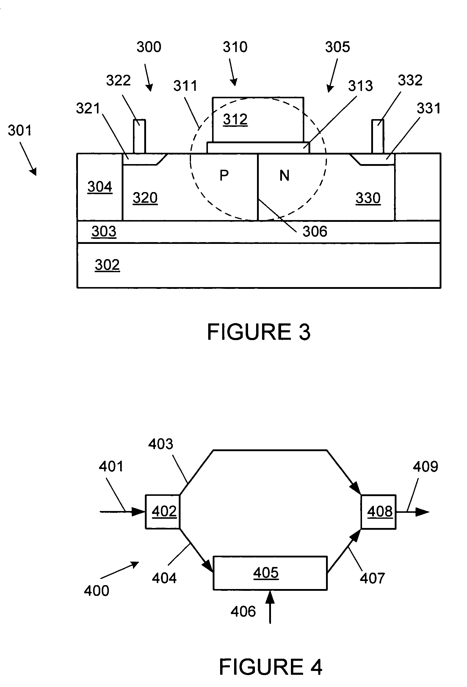
[0021]FIG. 1 is a cross sectional diagram, not to scale, of an integrated optical modulator, according to one embodiment of the present invention. Optical modulator 100 is made of lateral PN diode 105 fabricated across waveguide 110 on substrate 101. Substrate 101 in an exemplary embodiment is a SOI (silicon on insulator) substrate, made of silicon layer 104 on top of silicon dioxide layer 103, which is on top of silicon layer 102. Other types of substrates can be used, such as a five layer substrate made of three layers of silicon with two layers of silicon dioxide separating the silicon layers.
[0022]PN diode 105 has two doped regions 120 and 130, which are oppositely doped. The two doped regions 120 and 130 meet at PN junction 106. PN junction 106 is approximately in the center of waveguide 110 and in the approximate center of the optical mode, as shown by dashed line 111. Conductive plugs 122 and 132 connect to respective doped regions 120 and 130 via electrical contacts such as ...
PUM
| Property | Measurement | Unit |
|---|---|---|
| concentration | aaaaa | aaaaa |
| size | aaaaa | aaaaa |
| index of refraction | aaaaa | aaaaa |
Abstract
Description
Claims
Application Information