Bias voltage applying circuit and semiconductor memory device

a bias voltage and circuit technology, applied in the field of readout techniques, can solve the problems of affecting high-speed readout, deteriorating transient characteristics, increasing the bit line, etc., and achieve the effect of high-speed readout operation

Inactive Publication Date: 2006-08-08
SHARP KK
View PDF4 Cites 15 Cited by
  • Summary
  • Abstract
  • Description
  • Claims
  • Application Information

AI Technical Summary

Benefits of technology

[0020]In the bias voltage applying circuit according to the second aspect of the present invention, since the bias voltage applying circuit according to the first aspect of the present invention is implemented basically, the same effect can be provided. More specifically, since there can be provided a high gain output in each differential output of the bias voltage applying circuit because of the current mirror connection, there can be provided a gain output further higher than the normal current mirror connection.
[0023]In the bias voltage applying circuit according to the third aspect of the present invention, since the bias voltage applying circuit according to the first aspect of the present invention is implemented basically, the same effect can be provided. Further, since the bias voltage applying circuit according to the second aspect of the present invention is implemented basically, the same effect can be provided.
[0034]In the semiconductor memory device according to the first aspect of the present invention, there can be implemented a semiconductor memory device in which the effect of the bias voltage applying circuit according to the present invention is provided and high-speed readout operation can be performed.
[0036]In the semiconductor memory device according to the second aspect of the present invention, it is not necessary to select the bias circuit connected by the address of the selected memory cell using a particular selection circuit, and there can be provided constant readout performance regardless of the position of the selected memory cell in the main memory array.
[0038]In the semiconductor memory device according to the third aspect of the present invention, the transient response characteristics in both bit lines on the selected memory side and the reference memory cell side can be prevented from fluctuating and high-speed readout operation can be implemented.

Problems solved by technology

As a result, CR (capacity resistance product) of the bit line is increased and the transient characteristics deteriorates, which could hinder the high-speed readout.
Therefore, the current mirror operation is not correctly performed for the above period, which could hinder the high-speed readout.

Method used


Image

  • Bias voltage applying circuit and semiconductor memory device
  • Bias voltage applying circuit and semiconductor memory device
  • Bias voltage applying circuit and semiconductor memory device

Examples


first embodiment

[0051]A first embodiment of a semiconductor memory device and a bias voltage applying circuit according to the present invention (occasionally referred to as “inventive device” and “inventive circuit”, respectively, hereinafter) will be described with respect to the accompanying drawings.

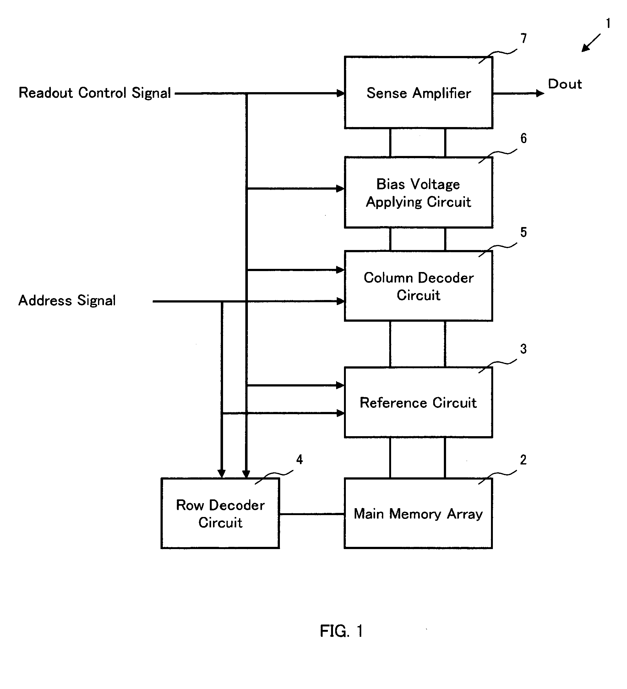
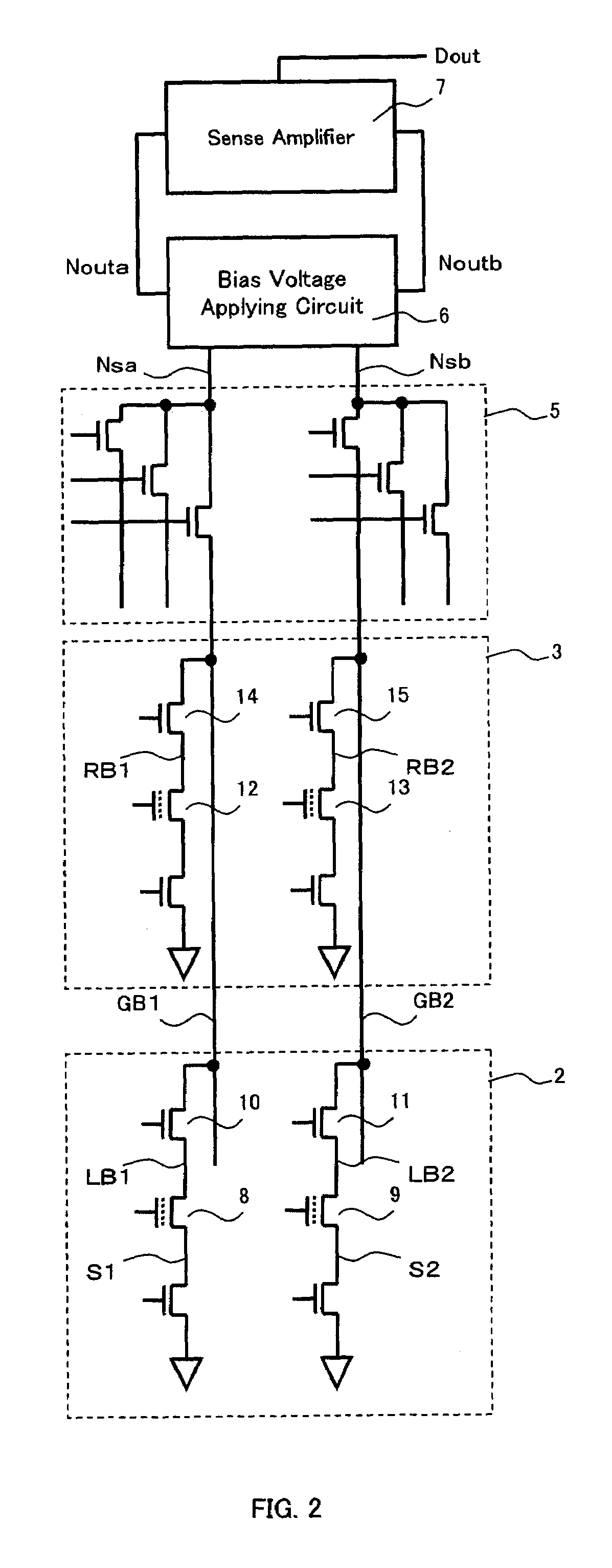
[0052]As shown in FIG. 1, an inventive device 1 comprises a main memory array 2, a reference circuit 3, a row decoder 4, a column decoder 5, a bias voltage applying circuit 6 according to the present invention, a sense amplifier 7 and the like. In addition, necessary address signal and a readout control signal (a chip enable signal, an output enable signal and the like) are input to each part through an input circuit although they are not shown. In addition, an output Dout of the sense amplifier 7 is output to an external circuit through a predetermined output circuit.

[0053]The main memory array 2 is so constituted that a plurality of memory cells to be read out are arranged in the row direction and...

second embodiment

[0072]Next, a circuit constitution and a circuit operation of a semiconductor memory device according to a second embodiment of the present invention will be described with reference to the drawings.

[0073]As shown in FIG. 11, an inventive circuit 6 of this embodiment comprises two bias circuits 30 which are entirely equivalent to each other. Similar to the first embodiment, one of them is referred to as a first bias circuit 30a and the other is referred to as a second bias circuit 30b for convenience. In addition, similar to the first embodiment, one of two current sources Ia and Ib designates a memory cell current Icell of the selected memory cell and the other designates a memory cell current Iref of the reference memory cell. The memory cell current Icell of the selected memory cell is changed depending on the threshold voltage corresponding to the storage information.

[0074]The bias circuit 30a (30b) of this embodiment comprises six active elements comprising MOSFETs. A first act...

third embodiment

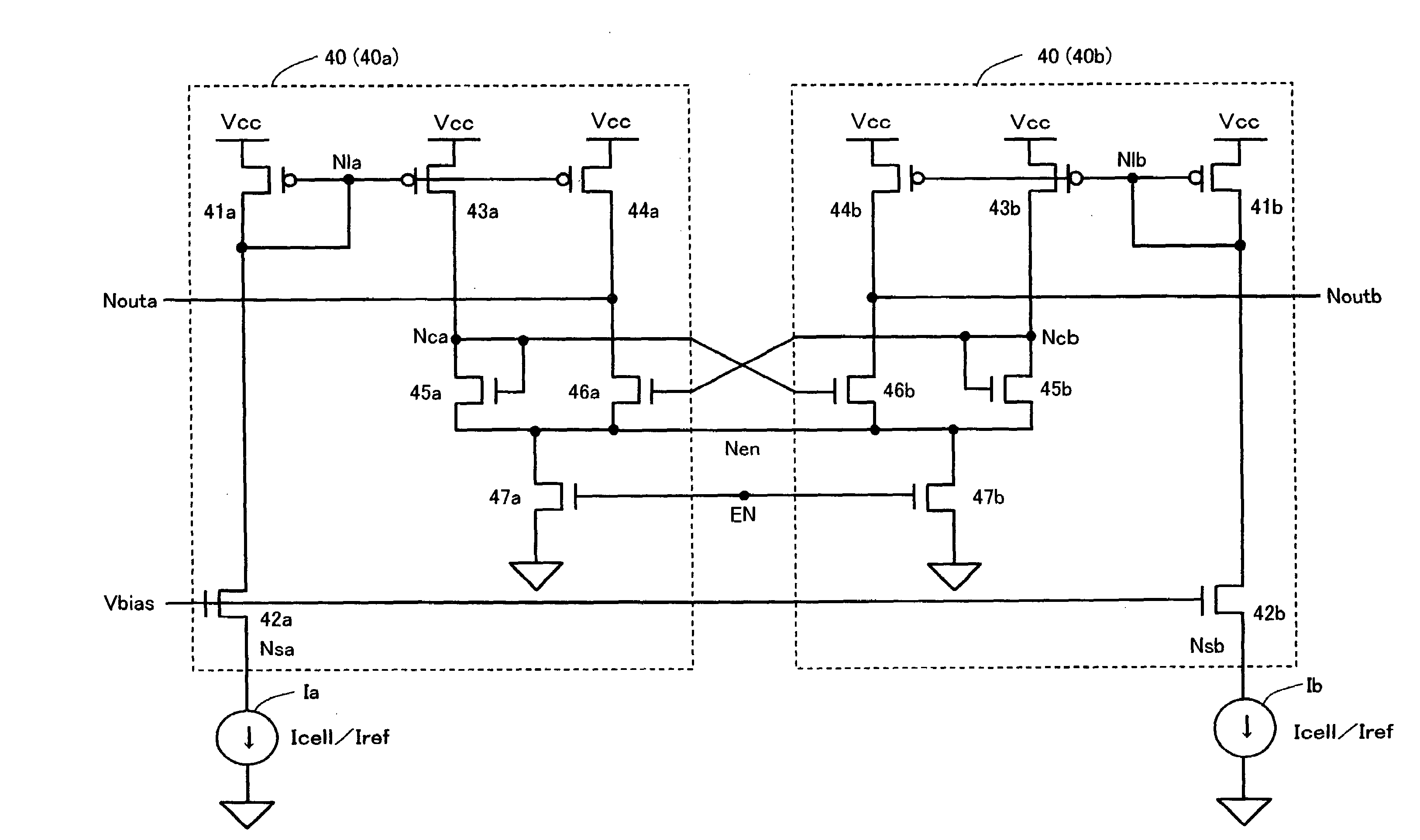
[0084]Next, a circuit constitution and a circuit operation of a semiconductor memory device according to a third embodiment of the present invention will be described with reference to the drawings. Although the current path of the memory cell current Icell or the reference memory cell current Iref which was copied from the first active element to the third active element is divided in the second embodiment, a current path is not divided in this embodiment and a current is copied from a first active element to a third active element and a fourth active element.

[0085]As shown in FIG. 12, an inventive circuit 6 of this embodiment comprises two bias circuits 40 which are entirely equivalent to each other. Similar to the first and second embodiments, one of them is referred to as a first bias circuit 40a and the other is referred to as a second bias circuit 40b for convenience. In addition, similar to the first and second embodiments, one of two current sources Ia and Ib designates a me...


PUM


Abstract

Two bias circuits which supply a current to a selected memory cell and a reference memory cell have the same circuit constitution. Each bias circuit includes a first active element between a power supply node and a junction node, where a current is controlled to prevent a voltage level at the junction node from fluctuating, a second active element between the power supply node and an output node, where a current is controlled such that a voltage level at the output node is changed in direction opposite to a voltage level at the junction node in other bias circuit, a third active element and a fourth active element between the junction node and a current supply node and between the output node and the current supply node, respectively, where a bias voltage is adjusted.

Description

CROSS REFERENCE TO RELATED APPLICATION[0001]This Nonprovisional application claims priority under 35 U.S.C. §119(a) on Patent Applications ser. No. 2004-031648 and No. 2004-349252 filed in Japan on Feb. 9, 2004 and on Dec. 2, 2004, respectively, the entire contents of which are hereby incorporated by reference.BACKGROUND OF THE INVENTION[0002]1. Field of the Invention[0003]The present invention relates to a semiconductor memory device and, more particularly, it relates to readout technique in which a current flowing in a memory cell of a semiconductor memory device is detected and its storage state is determined at high speed.[0004]2. Description of the Related Art[0005]There are various kinds of methods of reading out a storage state of a memory cell in a semiconductor memory device. A description will be made with reference to a flash memory which is one of a nonvolatile semiconductor memory device. The flash memory comprises a memory transistor in a memory cell having a floating ...

Claims


Application Information

Patent Timeline
Patent Type & Authority Patents(United States)
IPC IPC(8): G11C7/00G11C16/06G11C7/06G11C7/12G11C16/28G11C29/02
CPCG11C7/06G11C7/12G11C16/28G11C29/021G11C29/028G11C29/02G11C7/062G11C2207/063G11C2029/5004G11C5/14
Inventor MORI, YASUMICHIYOSHIMOTO, TAKAHIKOWATANABE, MASAHIKOANZAI, SHINSUKENOJIMA, TAKESHIMASAKI, MUNETAKA
Owner SHARP KK
Why Eureka
Try Eureka