Photonic crystal and producing method thereof

Inactive Publication Date: 2006-08-08
SHARP KK
View PDF3 Cites 9 Cited by
  • Summary
  • Abstract
  • Description
  • Claims
  • Application Information

AI Technical Summary

Benefits of technology

[0010]An object of the present invention is to provide a photonic crystal capable of efficient

Problems solved by technology

The conventional photonic crystals produced by the above-described methods and others, however, would pose a problem that external light is not introduced the

Method used


Image

  • Photonic crystal and producing method thereof
  • Photonic crystal and producing method thereof
  • Photonic crystal and producing method thereof

Examples


Example

First Embodiment

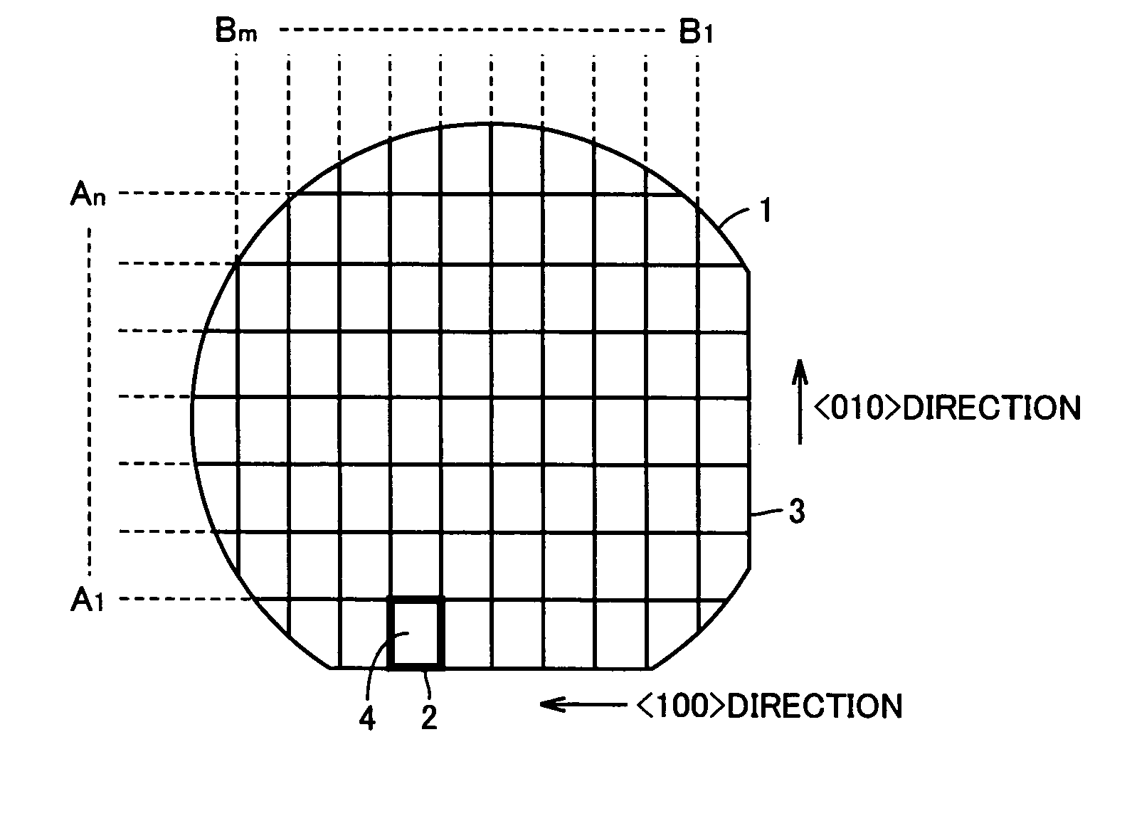
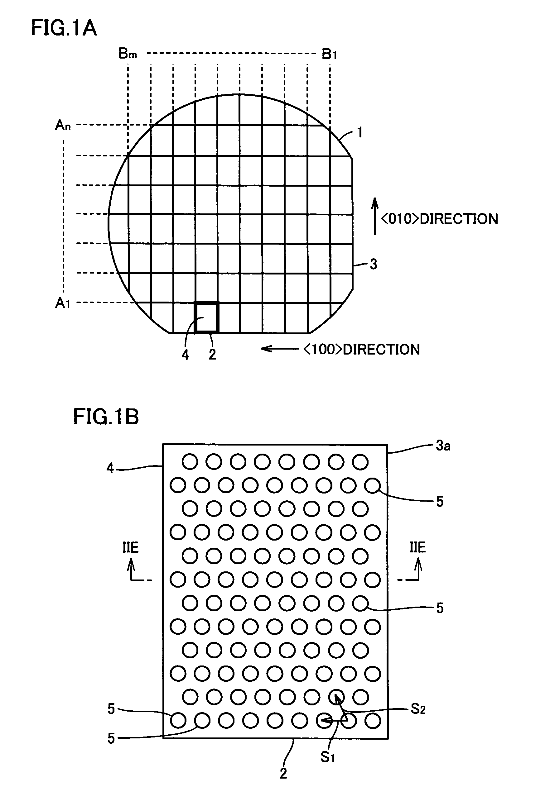
[0034]A preferable example of a wafer including photonic crystals according to a first embodiment of the present invention is shown in FIG. 1A in schematic top plan view. A preferable example of the photonic crystal of the first embodiment of the present invention is shown in FIG. 1B in schematic top plan view.

[0035]As shown in FIG. 1A, the wafer 1 including a plurality of photonic crystals 4 has cleaved surfaces 2 and 3 on its sides. Individual photonic crystals 4 obtained by cleaving wafer 1 each have a plurality of cylindrical holes 5 periodically arranged in the semiconductor, as shown in FIG. 1B. Holes 5 include the air therein. Photonic crystal 4 has cleaved surfaces 2 and 3a. Primitive translation vectors S1 and S2 may be adopted as the primitive translation vectors representing the periodic arrangement directions of the air within the semiconductor. Here, the direction of primitive translation vector S1 and cleaved surface 2 are made parallel to each other, b...

Example

Second Embodiment

[0050]The photonic crystal according to a second embodiment of the present invention is characterized in that the periodic arrangement pattern of the air within holes 5 forms a square lattice pattern as shown in a schematic enlarged top plan view of FIG. 4, instead of the triangular lattice pattern in the first embodiment.

[0051]The primitive translation vectors may be turned to the left by 45 degrees around hole 5a, to make the direction of a composite vector (β1+β2) of primitive translation vectors β1 and β2 in parallel with cleaved surface 2. When the primitive translation vectors are turned to the left additionally by 45 degrees, the direction of primitive translation vector β2 becomes parallel to cleaved surface 2. The other configuration of the second embodiment is identical to that of the first embodiment, and thus, description thereof is not repeated here.

Example

Third Embodiment

[0052]The photonic crystal according to a third embodiment of the present invention differs in producing method from those of the first and second embodiments. It also differs in that an oxide layer is formed between the air existing within the holes and the semiconductor substrate. A preferable example of the producing method of the photonic crystal according to the third embodiment is now explained.

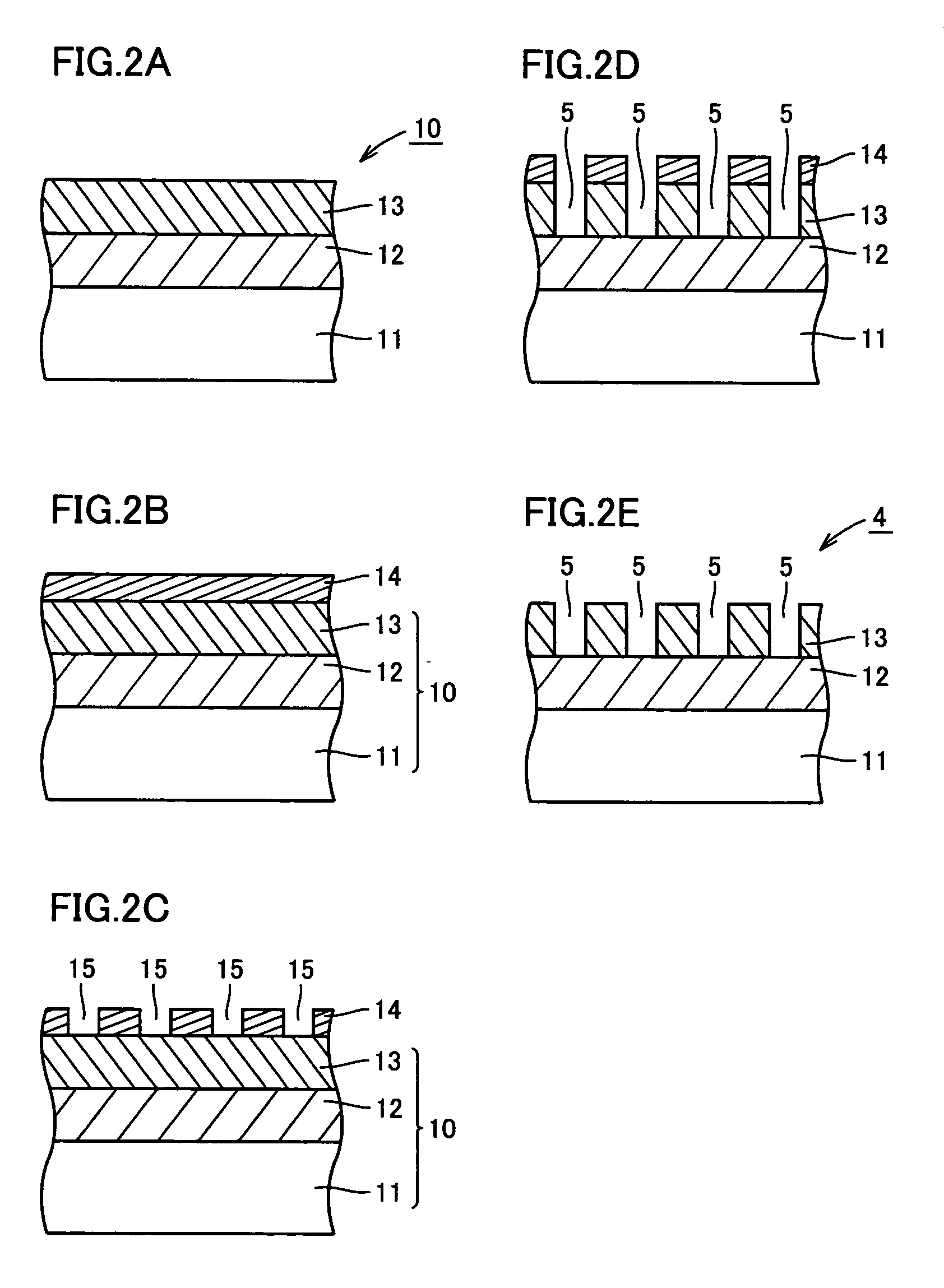
[0053]Firstly, as shown in a schematic enlarged cross section of FIG. 5A, a semiconductor substrate 11 of GaAs is prepared, and an oxide layer 22 of SiO2 is formed on semiconductor substrate 11 by electron beam evaporation or the like, to form a stack 20. Stack 20 is cleaved at its end to form a cleaved surface.

[0054]Next, photoresist 14 is applied on oxide layer 22, as shown in FIG. 5B. As shown in FIG. 5C, a plurality of openings 15 are formed in photoresist 14 in such a manner that the primitive translation vectors representing the periodic arrangement directions are ...


PUM


Abstract

A photonic crystal and a producing method thereof are provided. The photonic crystal includes at least two media of different refractive indices formed on a semiconductor substrate. One of the media is periodically arranged in another one of the media. The photonic crystal has a cleaved surface on its side. The directions of primitive translation vectors representing the periodic arrangement directions of the one medium are at desired angles with the cleaved surface. Preferably, the direction of at least one of the primitive translation vectors is in parallel with the cleaved surface.

Description

[0001]This nonprovisional application is based on Japanese Patent Application No. 2003-151137 filed with the Japan Patent Office on May 28, 2003, the entire contents of which are hereby incorporated by reference.BACKGROUND OF THE INVENTION[0002]1. Field of the Invention[0003]The present invention relates to a photonic crystal and a producing method thereof, and more particularly to a photonic crystal capable of efficiently introducing external light and producible with a high yield, and a producing method thereof. The term “light” herein is a concept including, not only visible light, but also electromagnetic waves of longer or shorter wavelengths than the visible light.[0004]2. Description of the Background Art[0005]In recent years, a photonic crystal of a multi-layered structure formed of at least two kinds of dielectric, semiconductor or other materials, having a periodic structure with the refractive index distributed periodically, has attracted an attention. In the photonic cry...

Claims


Application Information

Patent Timeline
IPC IPC(8): G02B6/02G02B6/00G02B6/10G02B6/28G02B6/32G02B6/36H01L21/00G02B6/12G02B6/122G02B6/13
CPCG02B6/1225B82Y20/00
Inventor KATOH, YOSHIMICHIOKUMURA, TOSHIYUKI
Owner SHARP KK
Why Eureka
Try Eureka