Integrated RF front end

a front end and integrated circuit technology, applied in low-noise amplifiers, gain control, substation equipment, etc., can solve the problems of consuming the most integrated circuit area, requiring extensive filtering of type outputs from such amplifiers, and most significant unintended or “spurious” emissions

Active Publication Date: 2006-08-08
PSEMI CORP
View PDF16 Cites 97 Cited by
  • Summary
  • Abstract
  • Description
  • Claims
  • Application Information

AI Technical Summary

Benefits of technology

[0011]A combination of methods and / or circuits is described that enables the fabrication of a self-protected monolithic integrated circuit including all of the RF front-end sections of a communications transceiver. Such self-protected RF front-end circuits particularly include those sections, from a Power Amplifier (PA) through an antenna connection, that permit efficient internal protection from overload due to an improper, missing or damaged antenna.

Problems solved by technology

Of these circuits, the PA subcircuit is typically the most power-consuming portion of such transmitters, and, also typically, is the source of the most significant unintended or “spurious” emissions.
Due to their need to handle high power, the PA and antenna switch subcircuits consume the most integrated circuit area.
Manufacturing costs for integrated circuits are strongly dependent on the amount of device area required for each circuit.
However, the pulse-type outputs from such amplifiers generally require extensive filtering in order to establish a narrow-band sinusoidal output, as is typically required.
While normal operation of PAs in classes D–F does not intentionally cause drive element devices to conduct while voltage is present across the devices, even switched devices consume real power due to current flowing while voltage is present during finite switching periods.
The higher frequency signals include significant energy at undesired frequencies, and such undesired signal energies not only consume circuit power, but also require filtering to meet emission limits.
However, integrated circuit (IC) FETs have a limited capability to withstand voltage between any two nodes, including gate-source, gate-drain, and drain-source node pairs.
Such voltage withstand limitations may particularly impair the usefulness of IC FETs in high power switching circuits, in which inductive voltages may greatly exceed the supply voltage.
One of the difficulties with existing PA technologies is that many otherwise desirably high-speed devices are fabricated using processes that tend to yield FETs having relatively low breakdown voltages.

Method used


Image

  • Integrated RF front end
  • Integrated RF front end
  • Integrated RF front end

Examples


Embodiment Construction

I. Power Amplifier Overview

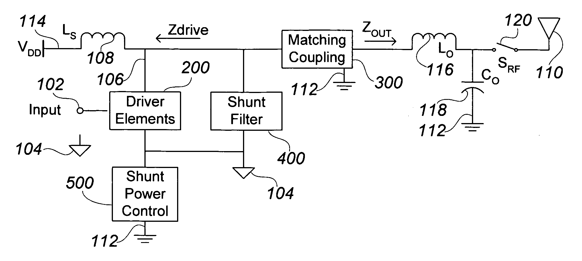
[0035]FIG. 1 is a block diagram of an RF power amplifier (PA). The illustrated RF PA is quite general, in that varying the biasing of devices in a driver elements block 200, and / or varying details of the other blocks, will permit the RF PA illustrated in FIG. 1 to operate in any of amplifier classes A, B, C, E, F, or, as described further herein, as an iClass amplifier. FIGS. 2–5 each show an exemplary circuit to implement one of the blocks shown in FIG. 1.

[0036]An input 102 is provided to the PA with respect to a circuit reference, or common, 104. The input 102 generally comprises a properly biased signal at a center drive frequency, f0. In response to the input 102, the driver elements block 200 controls conduction between a drive output node 106 and the circuit common 104. The driver elements block 200, in conjunction with current from VDD via an RF choke (RFC) LS 108, provides a signal having a particular impedance Zdrive. Zdrive may vary with frequenc...


PUM


Abstract

A monolithic integrated circuit (IC), and method of manufacturing same, that includes all RF front end or transceiver elements for a portable communication device, including a power amplifier (PA), a matching, coupling and filtering network, and an antenna switch to couple the conditioned PA signal to an antenna. An output signal sensor senses at least a voltage amplitude of the signal switched by the antenna switch, and signals a PA control circuit to limit PA output power in response to excessive values of sensed output. Preferred fabrication techniques include stacking multiple FETs to form switching devices. An iClass PA architecture is described that dissipatively terminates unwanted harmonics of the PA output signal. A preferred embodiment of the RF transceiver IC includes two distinct PA circuits, two distinct receive signal amplifier circuits, and a four-way antenna switch to selectably couple a single antenna connection to any one of the four circuits.

Description

[0001]This application is a continuation-in-part of co-pending and commonly assigned U.S. patent application Ser. No. 10 / 875,405, filed Jun. 23, 2004 and entitled “Stacked Transistor Method and Apparatus,” and is related to the following commonly owned U.S. patent documents: U.S. Pat. No. 5,663,570, issued Sep. 2, 1997 and entitled “High-Frequency Wireless Communication System on a Single Ultrathin Silicon On Sapphire Chip,” U.S. Pat. No. 6,804,502, issued Oct. 12, 2004 and entitled “Switch Circuit and Method of Switching Radio Frequency Signals,” and copending, published U.S. patent application Ser. No. 10 / 658,154, filed Sep. 8, 2003 and entitled “Low Noise Charge Pump Method and Apparatus;” and the contents of each of these four U.S. patent documents is hereby incorporated in its entirety by reference.BACKGROUND OF THE INVENTION[0002]1. Field of the Invention[0003]This invention relates broadly to integrated electronic circuits, and more specifically to RF transceiver circuitry.[0...

Claims


Application Information

Patent Timeline
Patent Type & Authority Patents(United States)
IPC IPC(8): H04B1/04H03F1/22H03F3/189H03F3/68H04B1/28H04M1/00
CPCH03F1/223H03F3/189H03F3/2171H03F3/68H03F2200/61H03F2200/294H03F2200/372H01Q23/00H03F1/565H03G3/3042H03G11/00H04B1/0475H04B1/48
Inventor BURGENER, MARK L.CABLE, JAMES S.
Owner PSEMI CORP
Why Eureka
Try Eureka