
Methods of and apparatus for pre-planarizing a substrate

a substrate and pre-planarization technology, applied in the field of semiconductor manufacturing, can solve the problems of current planarization techniques not being able to properly planarize such copper topography

Active Publication Date: 2006-08-15
LAM RES CORP
View PDF4 Cites 7 Cited by
  • Summary
  • Abstract
  • Description
  • Claims
  • Application Information

AI Technical Summary

Benefits of technology

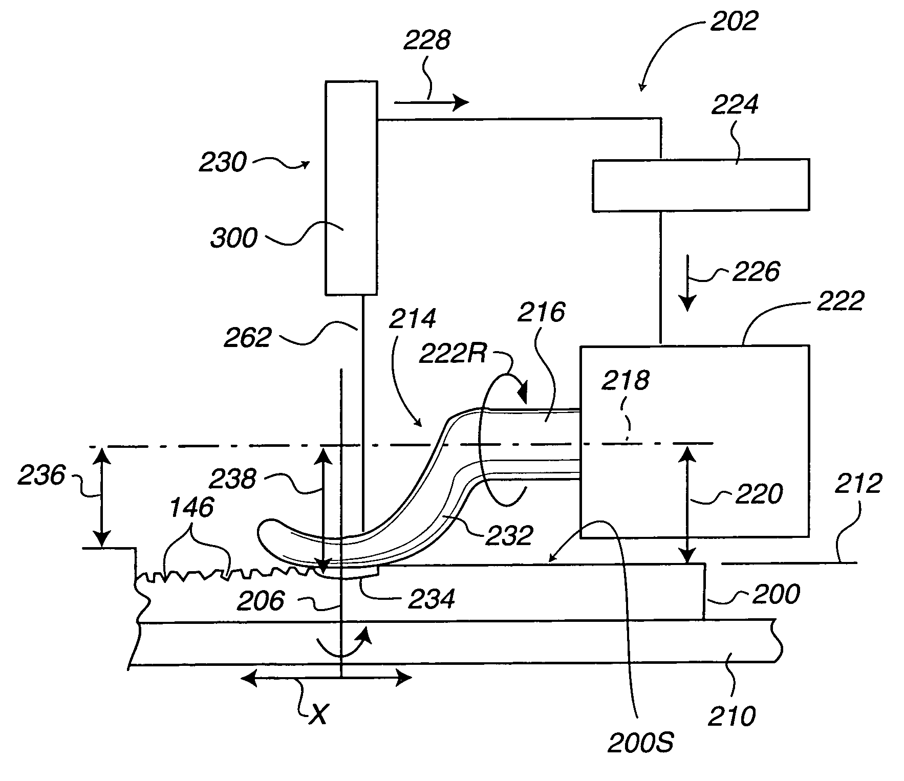
[0016]In another embodiment, the system may operate with the wafer having a wavy topography characterized by a contour from which a layer extends, the layer having an irregular thickness relative to the contour. The system may include a mount for rotating and traversing the wafer relative to the tool so that as the wafer rotates and traverses the planarization section contacts successive locations of the contoured topography of the wafer. The velocity of rotation of the planarization section around the axis of rotation is used to control the deflection of the planarization section within a predetermined range of values so that the planarization section follows the contour and removes portions of the layer to provide a pre-planarized substantially uniform layer thickness above the contour.
[0017]In another embodiment, a method of pre-planarizing a wafer is provided. The method may provide an operation of configuring a planarization tool with a shank defining an axis of rotation. The axis of rotation is spaced from the wafer by a first radial space having a first value. A planarization member is configured with a section coupled to the shank for rotation around the axis of rotation and located at an at-rest-position spaced by an at-rest-distance radially from the axis of rotation. The at-rest-distance has a second value that is less that the first value. The configuring of the section provides a flexure characteristic by which the planarization member responds to forces resulting from the radial spacing during the rotation, such that during the rotation the section flexes and the planarization member becomes located at a rotation-position spaced at a rotation-distance radially from the axis of rotation. A value of the rotation-distance is greater than the values of the at-rest-distance and the first value. The flexure characteristic is proportional to a velocity at which the planarization member rotates around the axis of rotation. The method may also control the velocity at which the planarization member rotates around the axis of rotation to selectively position the planarization member within the space between the tool and the wafer so that the planarization surface engages the wafer to perform a pre-planarization operation on the wafer.

Problems solved by technology

The topography resulting from the electroplating process may be referred to as the “copper topography”, and is not suitable to receive further layers without being planarized.
Current planarization techniques are not suited to properly planarize such copper topography resulting from the electroplating process.
For example, such planarization techniques are sensitive to pattern density and circuit layout.
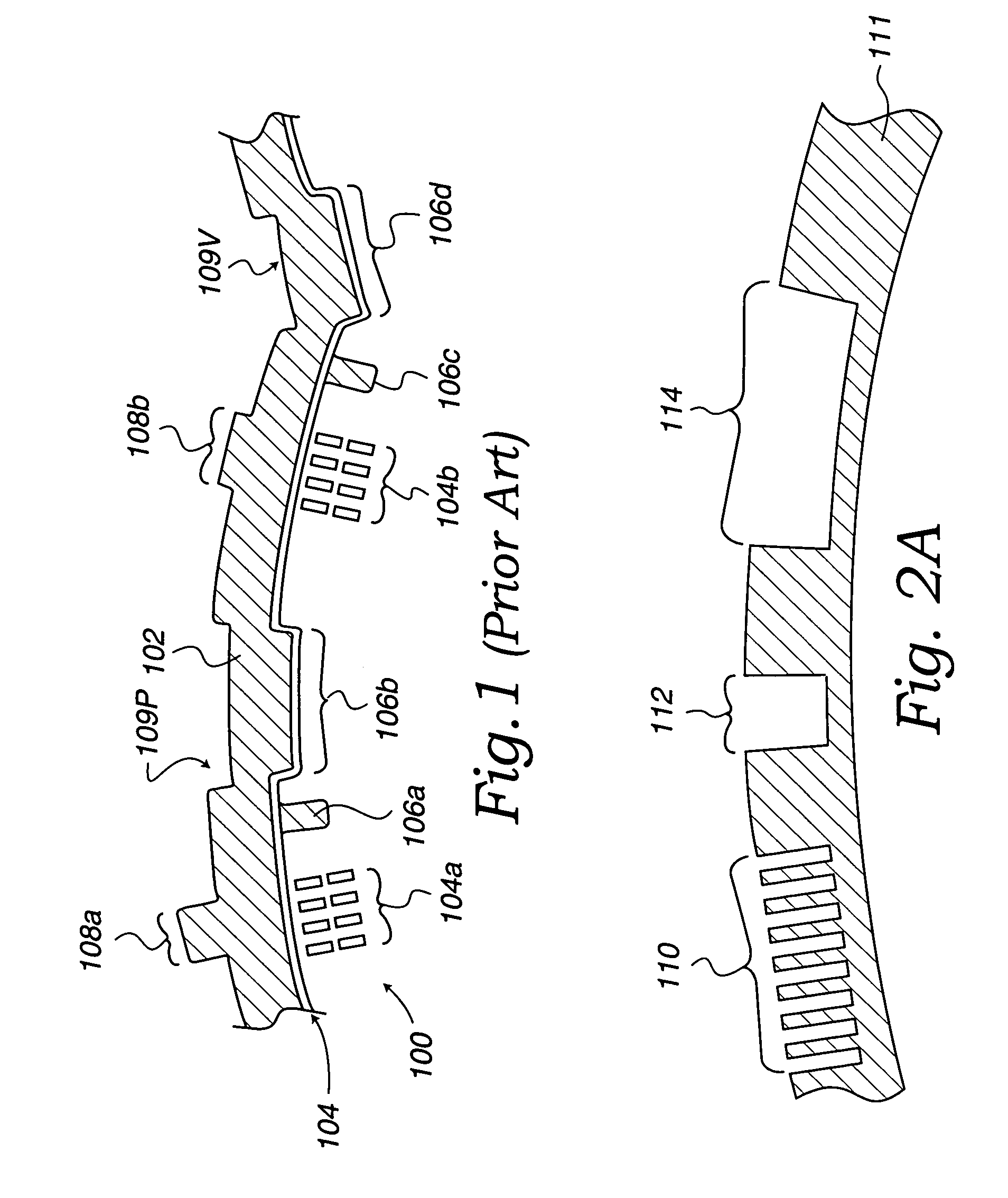
When attempting to perform a single CMP process on such copper topography without changing the consumables, attempts to completely remove the copper from regions 108a and 108b result in excessive dishing and erosion over trench regions 106a–d.
Current CMP processes do not suitably deal with both of these variables.
Another limitation of current CMP processes and related equipment is that the spindle that carries the wafer for processing is not designed for accurate Z axis motion.
Further, the effectiveness of existing metrology used to control such current CMP processing is limited to average measurements that extrapolate a measurement site to other sites that are not measured.
These include, for example, endless belts that engage the wafer and interfere with viewing or other monitoring of the planarizing activity by metrology apparatus.
Also, many CMP slurries are thick and not optically clear, for example, which tends to further interfere with viewing or other monitoring of the planarizing activity by the metrology apparatus.
Further, because the sensitivity (or resolution) required for following the wafer contour is in the submicron range of Z motion, stepping motors, for example, may possibly be inadequate for providing Z axis motion in submicron increments.
In any event, such motors, x-y stages and substrate chucks are relatively costly.

Method used


Image

  • Methods of and apparatus for pre-planarizing a substrate
  • Methods of and apparatus for pre-planarizing a substrate
  • Methods of and apparatus for pre-planarizing a substrate

Examples


Embodiment Construction

[0035]An invention is described for apparatus, methods, and a system for producing a normalized surface in preparation for a chemical mechanical planarization (CMP) process. It will be obvious, however, to one skilled in the art, that embodiments of the present invention may be practiced without some or all of these specific details. In other instances, well known process operations have not been described in detail in order not to obscure the present invention.

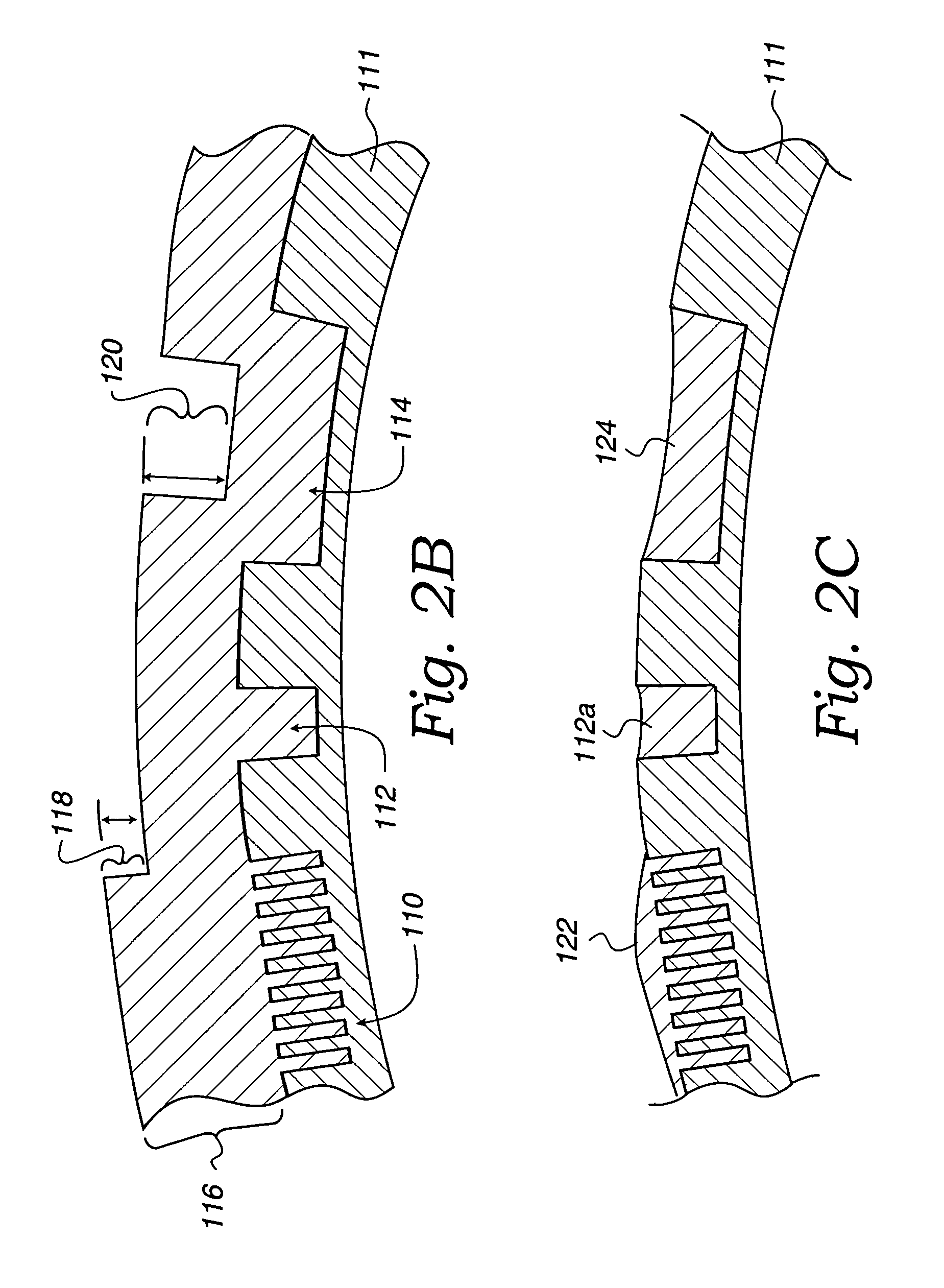
[0036]The embodiments of the present invention provide an apparatus, method, and system for performing a pre-planarization process in order to normalize a surface to be planarized. This normalization enables standardization of a subsequent planarization process. With this standardization, a number of benefits such as predictability, cost savings, etc., are realized. In one embodiment, the pre-planarization process is a process which scratches the top surface, e.g., a copper layer, of a copper topography of the substrate. As u...


PUM


Abstract

Methods and apparatus are provided to provide a substantially uniform layer thickness above a wafer contour as the wafer rotates and is traversed past a pre-planarization tool. The tool has a shank defining an axis of rotation, and a planarization member coupled to the shank has a hook-shaped section supporting a pre-planarization surface spaced by an at-rest-distance from the axis of during an at-rest condition of the shank. The hook-shaped section has a modulus of elasticity selected so that upon rotation, the hook-shaped section flexes and moves the pre-planarization surface to rotation-distances spaced from the axis in response to a velocity of rotation of the hook-shaped section around the axis in a range of velocities. As the tool rotates, metrology intermittently directly senses the layer thickness and controls the velocity of rotation so the rotation-distances have values in excess of a value of the at-rest-distance.

Description

BACKGROUND OF THE INVENTION[0001]1. Field of the Invention[0002]The present invention relates generally to semiconductor manufacturing and, more particularly, to methods of and apparatus for pre-planarizing a substrate in order to more efficiently perform a planarization operation.[0003]2. Description of the Related Art[0004]During copper interconnect manufacturing, a copper layer is deposited on a seed / barrier layer using an electroplating process. Components in the electroplating solution provide for appropriate gap fill on sub-micron features. However, these sub-micron features tend to plate faster than bulk areas and larger, i.e., greater than 1 μm, trench regions. Regions of the sub-micron features are typically found in large memory arrays such as, for example, static random access memory (SRAM). These array regions can comprise large areas of the wafer. The topography resulting from the electroplating process may be referred to as the “copper topography”, and is not suitable ...

Claims


Application Information

Patent Timeline
Patent Type & Authority Patents(United States)
IPC IPC(8): B24D17/00B24D99/00
CPCB24B7/228
Inventor BOYD, JOHN M.REDEKER, FRED C.DORDI, YEZDI
Owner LAM RES CORP
Learn More