
Method of making a trench MOSFET device with improved on-resistance

a technology of mosfet and trench, which is applied in the direction of semiconductor devices, basic electric elements, electrical equipment, etc., can solve the problems of increasing the risk of breakdown, and achieve the effects of improving on-resistance, improving on-resistance, and increasing design and process complexity

Inactive Publication Date: 2006-08-22
GEN SEMICON
View PDF8 Cites 6 Cited by
  • Summary
  • Abstract
  • Description
  • Claims
  • Application Information

AI Technical Summary

Benefits of technology

"The present invention provides a trench MOSFET device with improved on-resistance without substantially increasing design and process complexity. The device includes a substrate, an epitaxial layer, a trench, an insulating layer, a conductive region, a doped region, and a source region. The doped region is formed by a method that includes implanting a dopant and diffusing it at elevated temperature. The device also includes a trench bottom implant region that has a higher doping concentration than the surrounding drift region to reduce parasitic JFET. The invention also reduces resistance in the epitaxial layer between the trench bottoms and the substrate."

Problems solved by technology

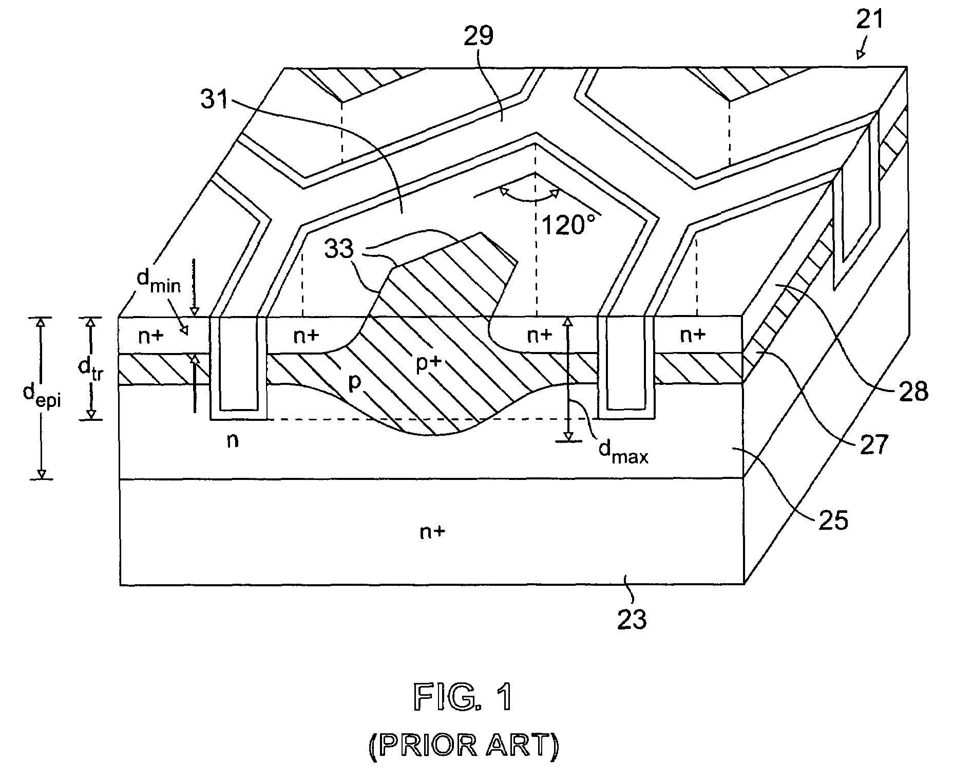
However, as is known in the art, the risk of breakdown increases as the epitaxial layer becomes thinner, particularly in the termination region, which is more vulnerable to breakdown.

Method used


Image

  • Method of making a trench MOSFET device with improved on-resistance
  • Method of making a trench MOSFET device with improved on-resistance
  • Method of making a trench MOSFET device with improved on-resistance

Examples


Embodiment Construction

[0020]The present invention now will be described more fully hereinafter with reference to the accompanying drawings, in which preferred embodiments of the present invention are shown. This invention may, however, be embodied in different forms and should not be construed as limited to the embodiments set forth herein.

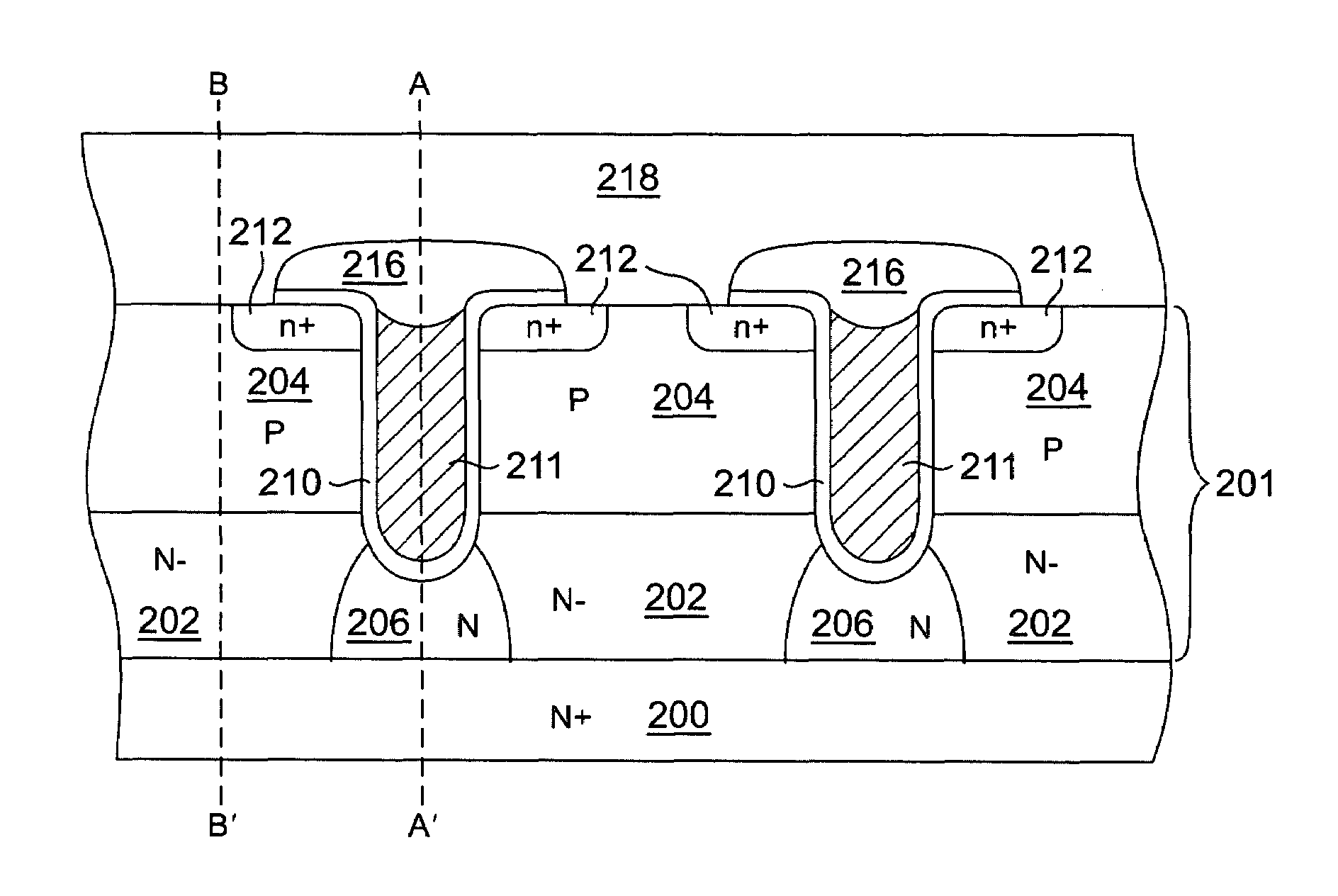
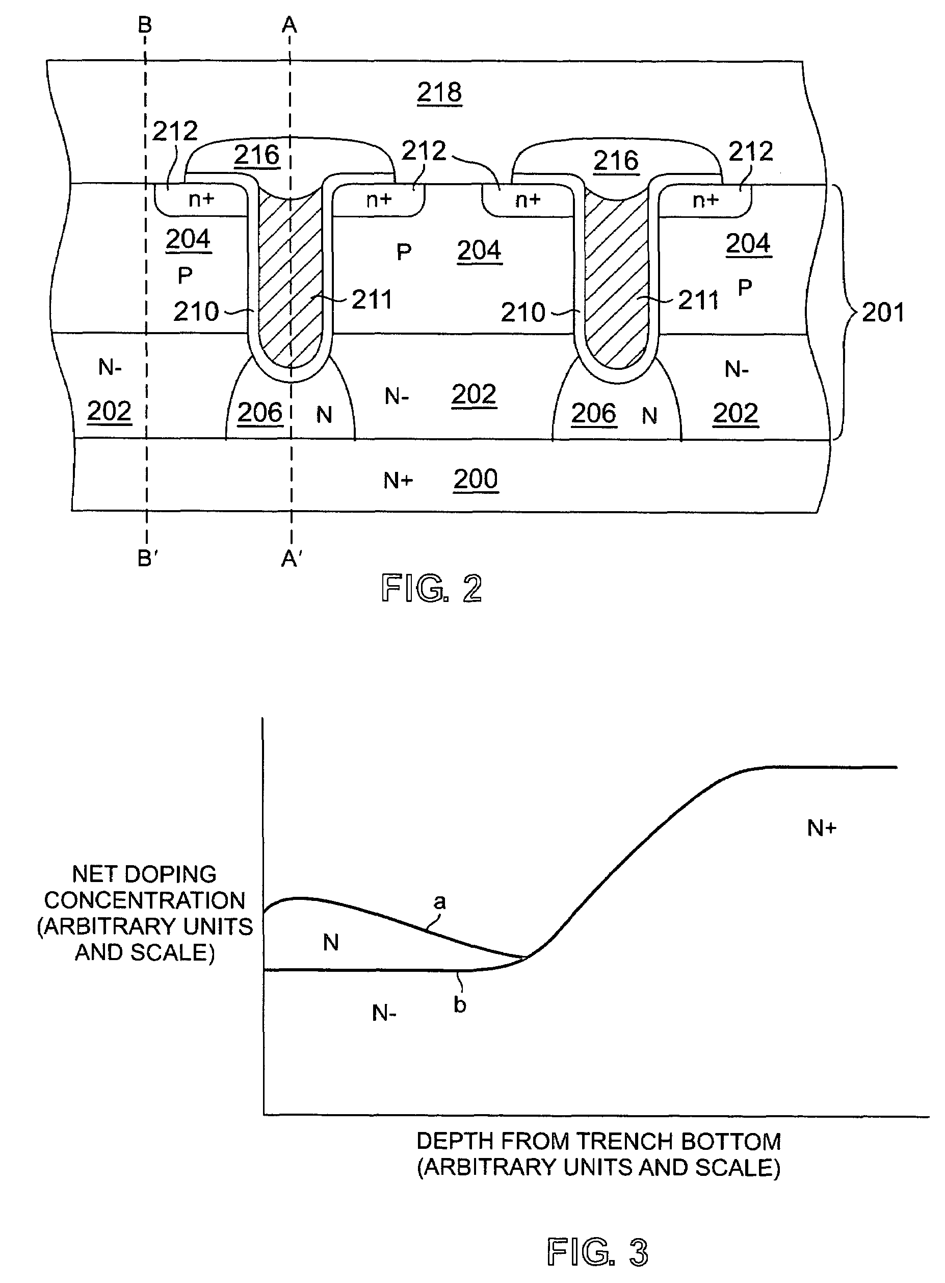
[0021]The present invention is directed to novel trench MOSFET structures in which a region of relatively high majority carrier concentration (sometimes referred to herein as a “trench bottom implant” based on its preferred mode of formation) is provided between the trench bottom and the substrate. One advantage associated with such a trench MOSFET structure is improved on-resistance.

[0022]FIG. 2 illustrates a trench MOSFET in accordance with an embodiment of the present invention. In the trench MOSFET shown, an epitaxial layer 201 is provided on an N+ substrate 200.

[0023]The N+ substrate 200 in this specific example is a silicon substrate having a thickness ranging, f...


PUM


Abstract

A method of forming a trench MOSFET device includes depositing an epitaxial layer over a substrate, both having the first conductivity type, the epitaxial layer having a lower majority carrier concentration than the substrate, forming a body region of a second conductivity type within an upper portion of the epitaxial layer, etching a trench extending into the epitaxial layer from an upper surface of the epitaxial layer, the trench extending to a greater depth from the upper surface of the epitaxial layer than the body region, forming a doped region of the first conductivity type between a bottom portion of the trench and substrate, the doped region having a majority carrier concentration that is lower than that of the substrate and higher than that of the epitaxial layer, wherein the doped region is diffused and spans 100% of the distance from the trench bottom portion to the substrate, forming an insulating layer lining at least a portion of the trench, forming a conductive region within the trench adjacent the insulating layer and forming a source region of said first conductivity type within an upper portion of the body region and adjacent the trench.

Description

STATEMENT OF RELATED APPLICATION[0001]This application is a division of U.S. patent application Ser. No. 09 / 999,116 entitled “Trench MOSFET Device With Improved On-Resistance,” filed on Nov. 21, 2001 now U.S. Pat. No. 6,657,254.BACKGROUND OF THE INVENTION[0002]The present invention relates to trench MOSFET devices, and more particularly to trench MOSFET devices with improved on-resistance.[0003]A trench MOSFET (metal-oxide-semiconductor field-effect transistor) is a transistor in which the channel is formed vertically and the gate is formed in a trench extending between the source and drain. The trench, which is lined with a thin insulator layer such as an oxide layer and filled with a conductor such as polysilicon (i.e., polycrystalline silicon), allows less constricted current flow and thereby provides lower values of specific on-resistance. Examples of trench MOSFET transistors are disclosed, for example, in U.S. Pat. Nos. 5,072,266, 5,541,425, and 5,866,931, the disclosures of w...

Claims


Application Information

Patent Timeline
Patent Type & Authority Patents(United States)
IPC IPC(8): H01L21/8238H01L21/336H01L29/08H01L29/78
CPCH01L29/7813H01L29/0878H01L29/66734H01L21/02521H01L21/0455H01L29/7812H01L2924/13091
Inventor HSHIEH, FWU-IUANSO, KOON CHONGAMATO, JOHN E.TSUI, YAN MAN
Owner GEN SEMICON
Learn More