Carbon nanotube interconnect

Inactive Publication Date: 2006-08-22
NASA +1
View PDF23 Cites 94 Cited by
  • Summary
  • Abstract
  • Description
  • Claims
  • Application Information

AI Technical Summary

Benefits of technology

[0008]This process supports CNT aspect ratios of 100:1 and higher, a variety of CNT array patterns, nearest neighbor CNT spacings of between 30 nm and 10 μm, current den

Problems solved by technology

MPs require local, intermediate and global wiring solutions and present both material and processing difficulties.
Susceptibility of common interconnect metals t electromigration at high current densities (above 106 Amp/cm2) is a problem.
However, electrical resistivity of copper increases with decreasing dimensions and is attributed to scattering at surfaces and at grain boundaries.
These size effects are due to interface roughness and by use of small grain sizes, which

Method used


Image

  • Carbon nanotube interconnect
  • Carbon nanotube interconnect
  • Carbon nanotube interconnect

Examples


Embodiment Construction

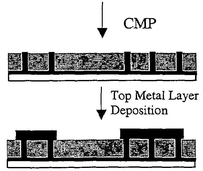
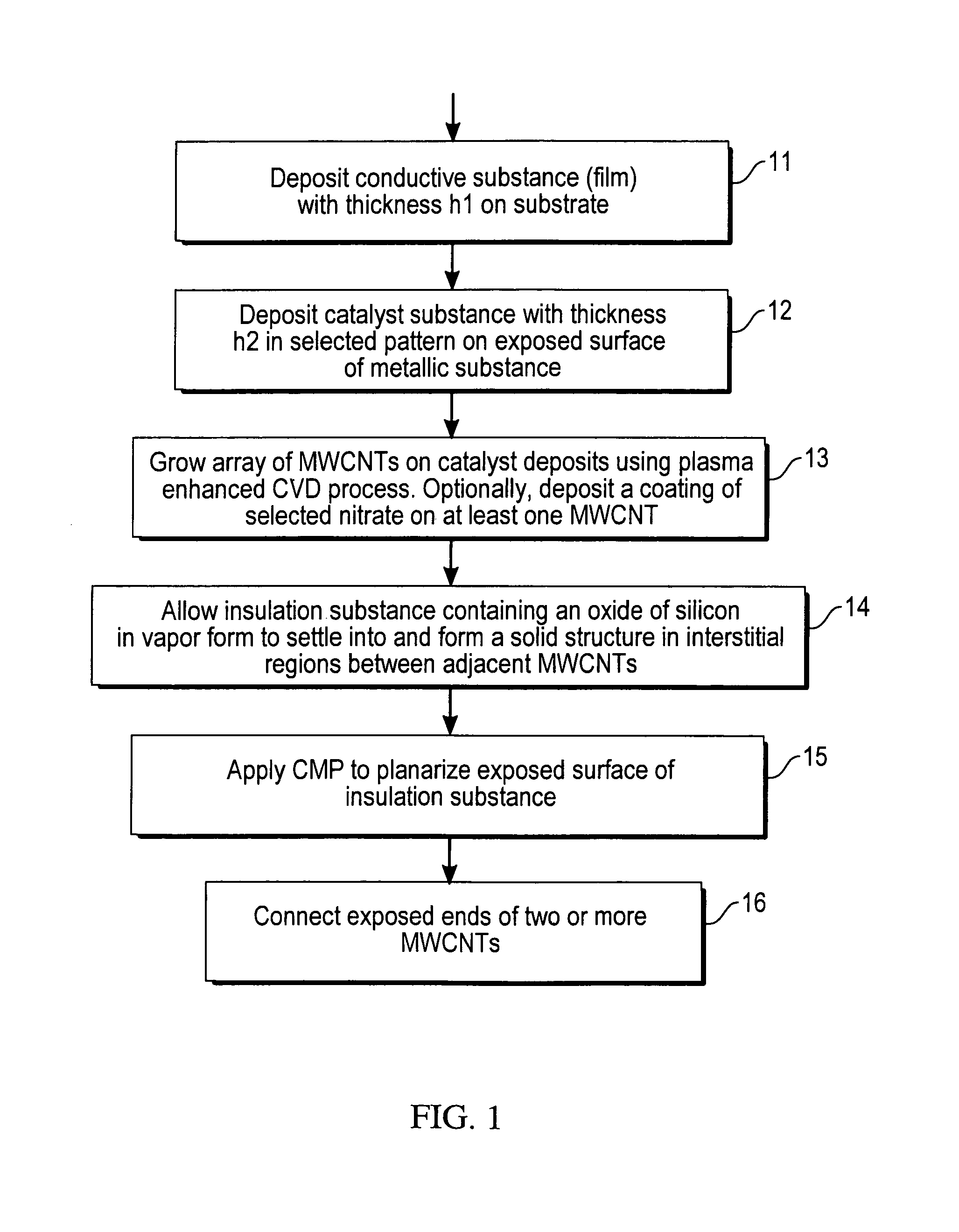
[0018]FIG. 1 is a flow chart of a procedure for fabricating an electrical interconnect according to one embodiment of the invention. In step 11, a selected conductive substance, having a conductive substance (film) first selected thickness h1 in a range 1 nm≦h1≦2 μm, or greater if desired, is deposited on a selected substrate. The substrate material may include a silicon oxide, SiOx, a selected nitride, SiyNz, or another suitable insulating material, of thickness 200–500 nm or greater, on an Si wafer. The conductive substance may be Al, Mo, Cr, Ti, Ta, Pt, Ir or doped Si. A careful choice of the conductive substance (e.g., Mo, Cr or Ti) will eliminate or suppress diffusion of carbon within or through the conductive substance layer.

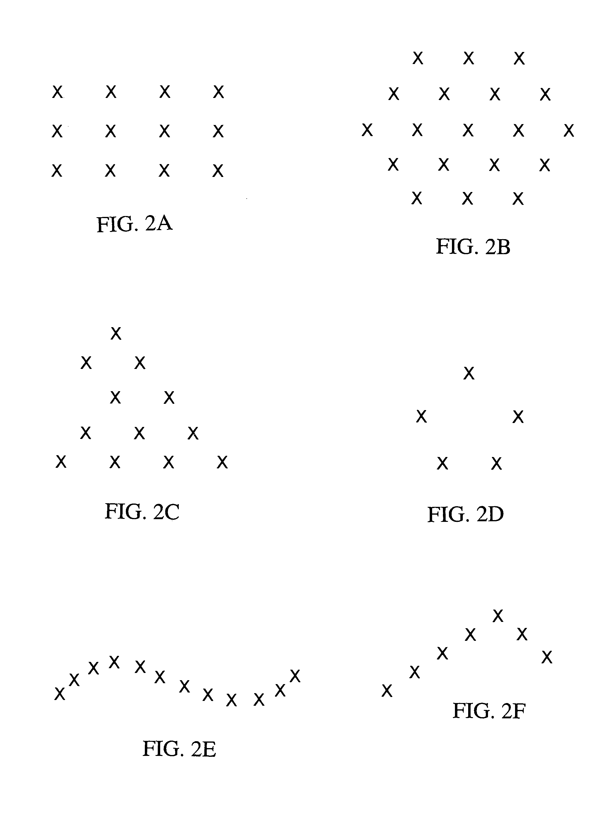
[0019]In step 12, a selected catalyst substance, such as Ni, Fe or Co, is deposited in a selected pattern, with a second thickness h2 in a range 1 nm≦h2≦30 nm, or higher if desired, on an exposed surface of the conductive substance. The selected pattern or...


PUM


Abstract

Method and system for fabricating an electrical interconnect capable of supporting very high current densities (106–1010 Amps/cm2), using an array of one or more carbon nanotubes (CNTs). The CNT array is grown in a selected spaced apart pattern, preferably with multi-wall CNTs, and a selected insulating material, such as SiOw or SiuNv, is deposited using CVD to encapsulate each CNT in the array. An exposed surface of the insulating material is planarized to provide one or more exposed electrical contacts for one or more CNTs.

Description

ORIGIN OF THE INVENTION[0001]The invention described herein was made in the performance of work under a NASA contract and is subject to the provision of Section 305 of the National Aeronautics and Space Act of 1958, Public Law 85-568 (72 Atat. 435; 42 U.S.C. 2457).FIELD OF THE INVENTION[0002]This invention relates to use of carbon nanotubes (CNTs) as interconnects for integrated circuit (IC) manufacturing.BACKGROUND OF THE INVENTION[0003]An interconnect in an integrated circuit distributes clock, regulatory and other signals as well as power or ground voltages to various components and circuits on a chip. The International Technology Roadmap for Semiconductors (ITRS) emphasizes the high speed transmission requirements on a chip as the driver for future interconnect development. Near term and long term interconnect requirements for microprocessors (MPs) and for dynamic random access memories (DRAMs) are outlined in the ITRS. MPs require local, intermediate and global wiring solutions...

Claims


Application Information

Patent Timeline
IPC IPC(8): H01L21/4763H01L21/302
CPCH01L21/76885H01L23/53276H01L2221/1094Y10S977/843H01L2924/0002Y10S977/842H01L2924/00
Inventor LI, JUNMEYYAPPAN, MEYYA
Owner NASA
Why Eureka
Try Eureka