Flat panel display device

a display device and flat panel technology, applied in the field of flat panel display devices, can solve the problems of difficult to secure spaces ranging across plural pixels, degradation of light emission properties of phosphors charged by charge accumulation, etc., to reduce thermal deformation influences, reduce the degradation of light emission properties of phosphors, and reduce the charging of phosphors

Inactive Publication Date: 2006-08-22
MAXELL HLDG LTD
View PDF12 Cites 6 Cited by
  • Summary
  • Abstract
  • Description
  • Claims
  • Application Information

AI Technical Summary

Benefits of technology

[0008]The present invention has been made in view of the above-described problem, and it is an object of the present invention to provide a flat panel display device capable of reducing charge accumulation on phosphors and locating spacers accurately and easily.
[0010]Since the metal sheet is electrically conductive, charges accumulated on phosphors are led toward the metal sheet via wall surfaces of the fine holes in contact with the phosphors. Consequently, the configuration in accordance with the present invention is capable of reducing the charging of the phosphors, and thereby reducing the degradation in light emission properties of the phosphors.
[0011]In the above-mentioned display substrate, a low-melting-temperature glass layer may be used as an adherent layer for affixing the above-mentioned metal sheet to the light-transmissive substrate, and materials of the metal sheet, the light-transmissive substrate and the glass layer may be selected to be approximately equal in coefficient of thermal expansion to each other. This configuration can reduce influences of thermal deformation caused among the metal sheet, the light-transmissive substrate and the glass layer.
[0012]Further, it is preferable to blacken a light-transmissive-substrate-side surface of the metal sheet approximately black, and this makes it possible to use the black surface of the metal sheet as a black matrix and to assemble the support members accurately and easily without degrading contrast ratio. Blackening can be carried out by blackening the metal sheet fabricated from an Fe—Ni alloy, or by coating black pigments on the metal sheet.
[0013]Further, recesses may be formed in the metal sheet for holding the spacers therein. The recesses facilitate positioning of the spacers in fitting the spacers to the metal sheet. This makes it possible to position the spacers by inserting ends of the spacers into the recesses in the metal sheet, and thereby to assemble the spacers accurately and easily.

Problems solved by technology

In the FED, light is generated by phosphors struck by electrons from cold cathodes, and therefore a problem arises in that phosphors charged by charge accumulation suffer from degradation in light emission properties.
Consequently, it is difficult to secure spaces ranging across plural pixels for forming the above-mentioned recesses by avoiding the bus interconnection layers.

Method used


Image

  • Flat panel display device
  • Flat panel display device
  • Flat panel display device

Examples


Embodiment Construction

[0019]The preferred embodiments in accordance with the present invention will be explained by reference to the drawings.

[0020]The following will explain examples of a flat panel display device of the present invention will be explained in detail by reference to FIGS. 1–5(c).

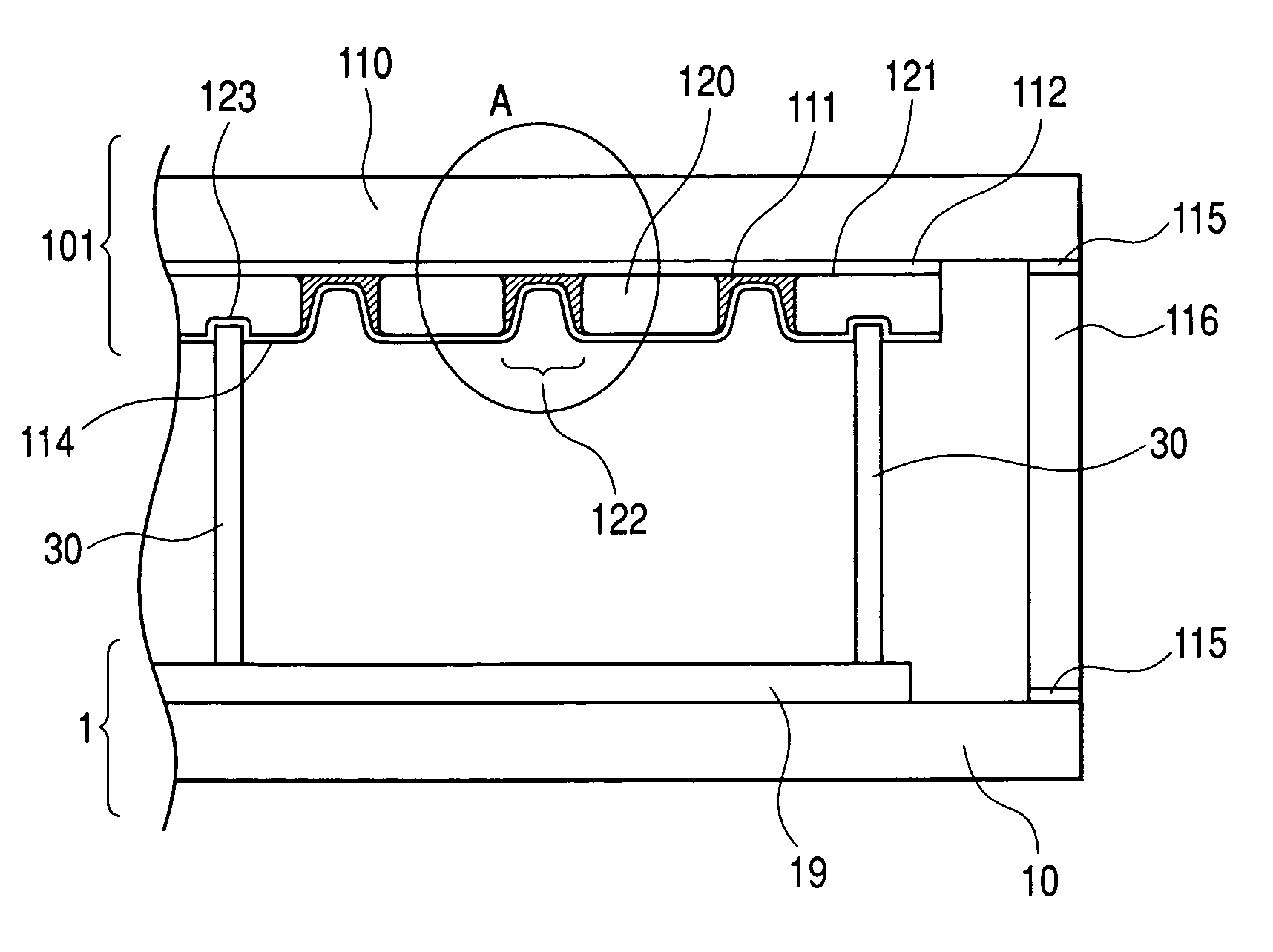
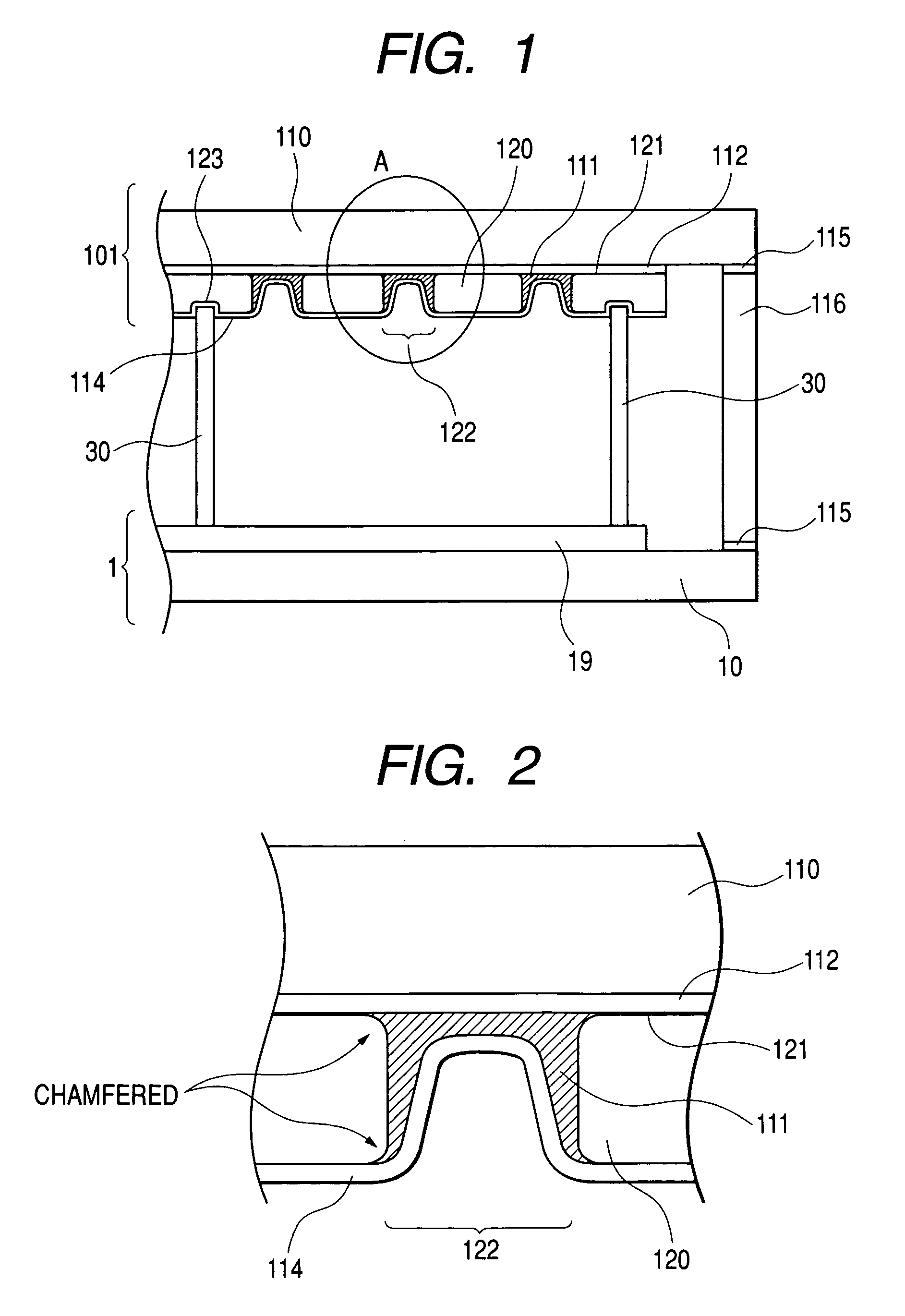
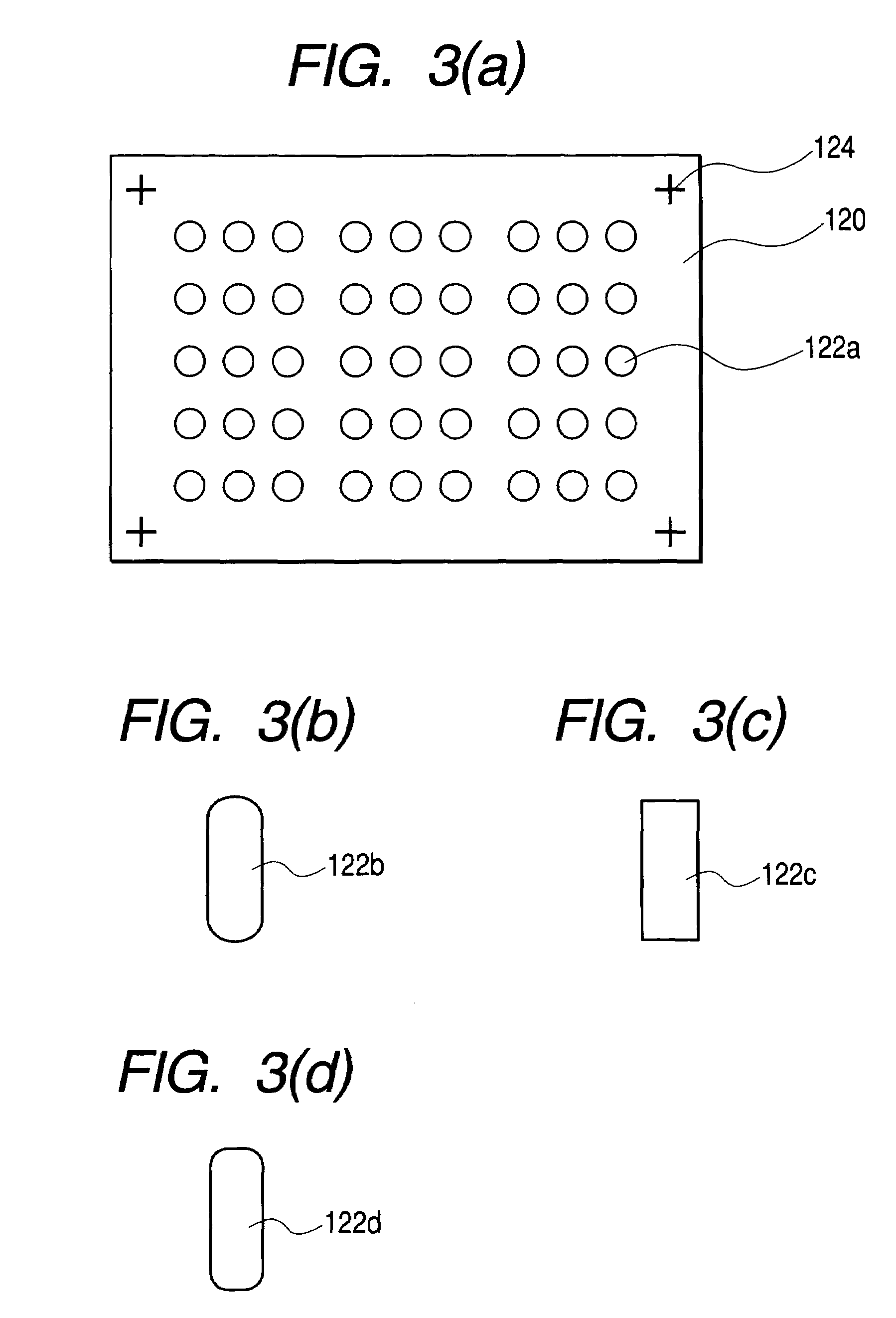
[0021]FIG. 1 illustrates a schematic configuration of a flat panel display device in accordance with an embodiment of the present invention. FIG. 2 is an enlarged detailed view of a portion designated A of FIG. 1. FIG. 3(a) is a top view of a metal sheet, and FIGS. 3(b)–3(d) are plan views of other examples of the shape of fine holes in the metal sheet, respectively. FIGS. 4(a)–4(c) illustrate examples of a metal sheet provided with recesses, FIG. 4(a) is a top view of one of the examples, FIG. 4(b) is a cross-sectional view of the metal sheet of FIG. 4(a), and FIG. 4(C) is a top view of the other examples of the two. FIGS. 5(a) and 5(b) are top views of other two examples of a metal sheet provided with recesses,...


PUM


Abstract

A flat panel display device capable of reducing charging of phosphors and disposing spacers easily and accurately. The flat panel display device has a rear substrate including an insulating substrate provided with many cold cathode elements for emitting electrons, a display substrate including a light-transmissive substrate disposed to face the rear substrate, and phosphors disposed on the light-transmissive substrate for generating light when excited by electron beams from the cold cathode elements, and a peripheral frame member. Provided on the light-transmissive substrate is a metal sheet perforated with plural fine holes arranged in a matrix configuration and having the phosphors disposed therewithin to form a light-emissive region.

Description

BACKGROUND OF THE INVENTION[0001]The present invention relates to a flat panel display device, and in particular to a field emission display (hereinafter FED), a flat panel display device incorporating in a hermetic container an electron source comprising a large number of cold cathode elements arranged in a matrix configuration for emitting electrons.[0002]Known as electron emitting elements for use in FED are surface conduction type emission element (hereinafter SED type), field emission type (hereinafter FE type) and metal-insulator-metal type emission element (hereinafter MIM type). Among the FE type, there are the Spindt type made up chiefly of a metal such as Mo and a semiconductor material such as Si and the CNT (Carbon Nanotube) type using carbon nanotubes as its electron source. The SED type is disclosed in Japanese Patent Application Laid-Open No. 2000-164129, for example, and the MIM type is disclosed in Japanese Patent Application Laid-Open Nos. 2001-101965 and 2001-2439...

Claims


Application Information

Patent Timeline
Patent Type & Authority Patents(United States)
IPC IPC(8): H01J63/04H01J29/87H01J1/30H01J29/08H01J29/24H01J29/32H01J31/12
CPCH01J31/127H01J29/085H01J1/30
Inventor OHISHI, TETSUSAGAWA, MASAKAZUKODERA, YOSHIEMIYATA, MOTOYUKIMAEDA, AKINORI
Owner MAXELL HLDG LTD
Why Eureka
Try Eureka