Efficient word recognizer for a logic analyzer

a logic analyzer and word recognition technology, applied in the field of logic analyzers, can solve the problems of increasing the length of the lead time, increasing the cost of the logic analyzer, and reducing the flexibility of the user, so as to achieve economic cost and retain a large measure of user flexibility

Inactive Publication Date: 2006-08-22
HEWLETT PACKARD DEV CO LP
View PDF1 Cites 5 Cited by
  • Summary
  • Abstract
  • Description
  • Claims
  • Application Information

AI Technical Summary

Benefits of technology

[0016]The problems noted above are solved in large part by one or more on-chip logic analyzers that include one or more word recognizers that can be programmed by a user to monitor a variety of values and conditions regarding the internal state data of the chip. The word recognizer accommodates a great deal of flexibility to allow various conditions and events to be combined together and compared separately or in conjunction to initiate storage of state data, while consuming a relatively small amount of space in the chip. The word recognizer can be implemented with a minimum of logic, and thus consumes relatively little pace on the chip. The word recognizer is configured in two portions. The first portion comprises a Boolean logic section that enables the user to specially configure the match conditions that will trigger data acquisition and / or data storage in an on-chip memory device. The second portion of the word recognizer comprises a counter / timer, which permits the user to count the number of times a match condition occurs, or the amount of time that the match condition exists (either for a single match condition, or cumulatively for all match conditions).
[0019]The present invention permits the incorporation of a relatively powerful word recognizer in an on-chip logic analyzer by constructing the word recognizer with some relatively basic Boolean functions, such as AND and OR gates, and some selection logic. The use of these simple gates, instead of a full-featured programmable logic device, permits the word recognizer to be designed in an extremely small space, at a very economical cost, thereby making it possible to include it on-chip. The word recognizer permits the recognition of both hardware and software terms, and retains a large measure of user flexibility in defining the conditions of interest.

Problems solved by technology

The design and development of digital logic circuits has become increasingly complex, due in large measure to the ever-increasing functionality offered in such circuits.
As integrated circuits become more complex, the length of the increases, requiring a greater lead-time before product release.
In addition, as the complexity of integrated circuits increase, it becomes necessary to fabricate more prototype iterations of the silicon (or “spins” of silicon) in order to remove successive layers of bugs from the design, thereby increasing the engineering and material cost of the released product.
One of the chief difficulties encountered during the debug phase of a product is identifying the source of an error, and obtaining relevant data regarding the conditions existing at the time of the error.
This can be extremely difficult because the error may make it impossible to obtain state information from the integrated circuit.
For example, in a processor, an error may cause the processor to quit executing, thus making it impossible to obtain the state data necessary to identify the source of the error.
As a result, the debug process often unfortunately requires that the debug team infer the source of the error by looking at external transactions at the time of the error, instead of being able to look at the internal state data.
Unfortunately, merely adding a soldered wire to a terminal or trace can create signal reflections, which may distort the data being monitored.
Thus, the manual probing of bus terminals and traces is impractical and inaccurate, especially those attached to high speed, highly complex chips.
More sophisticated techniques are also used, but are expensive and suffer, albeit to a lesser degree, from the same effects.
Both of these factors make it practically impossible to probe internal terminals of the chip or internal wire traces.
Moreover, to the extent that certain internal terminals and traces could be probed, the conventional methods for conducting such a probing operation are extremely expensive, and some might potentially corrupt the state of the terminals and traces being probed.
This approach, however, suffers in several respects.
Second, routing the desired state to external terminals often requires more wiring, silicon, drivers, pads and power than is affordable.
Attempts to do so can compromise the normal functioning of the chip.
And costs escalate throughout the design, often impacting the micropackaging and system board as well as the die.
Third, oftentimes the internal clock rate of the chip operates at a much higher rate than the external logic analyzers that receive and process the data.
The fastest commercial logic analyzers, despite their expense, are incapable of operating at GHz frequencies.
This solution, however, makes it more difficult to detect the bugs and errors that occur when the chip is running at full clock speeds.
The problem with this approach, however, is that it requires the allocation of a significant amount of chip space to incorporate such dedicated memory devices, and these memory devices, while used extensively during the design and development phase of the chip, add little or nothing to the performance of the chip once it is released into production.
Thus, the inclusion of dedicated memory space on the chip represents an opportunity cost, and means that functionality and / or performance is sacrificed to include this dedicated memory on the chip.
Consequently, the inclusion of memory for debug purposes, while helpful in the debug and test phase, is generally viewed as undesirable because of the accompanying loss of performance and functionality that must be sacrificed.
In relative terms, the largest dedicated on-chip memories typically are incapable of storing very much data.
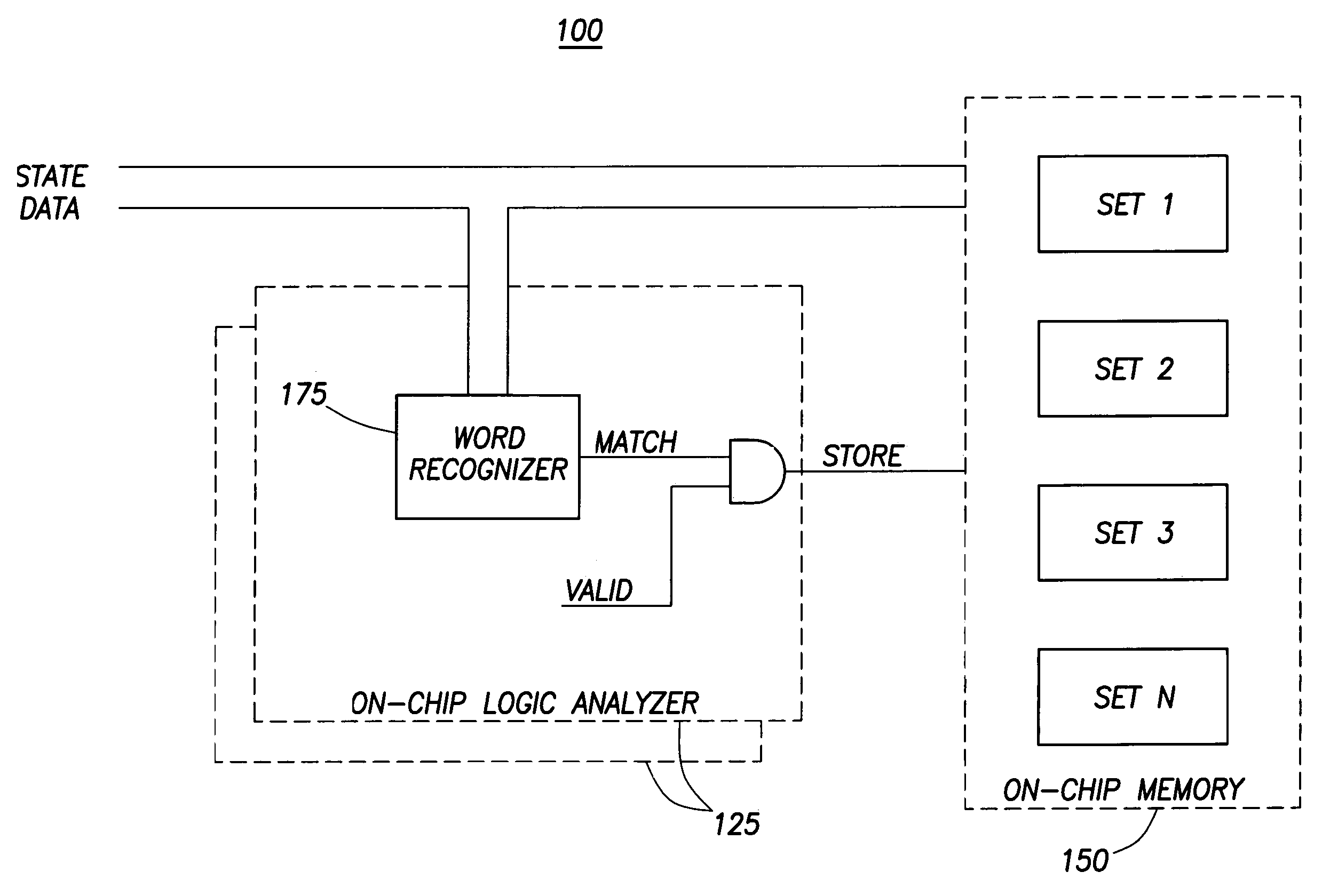
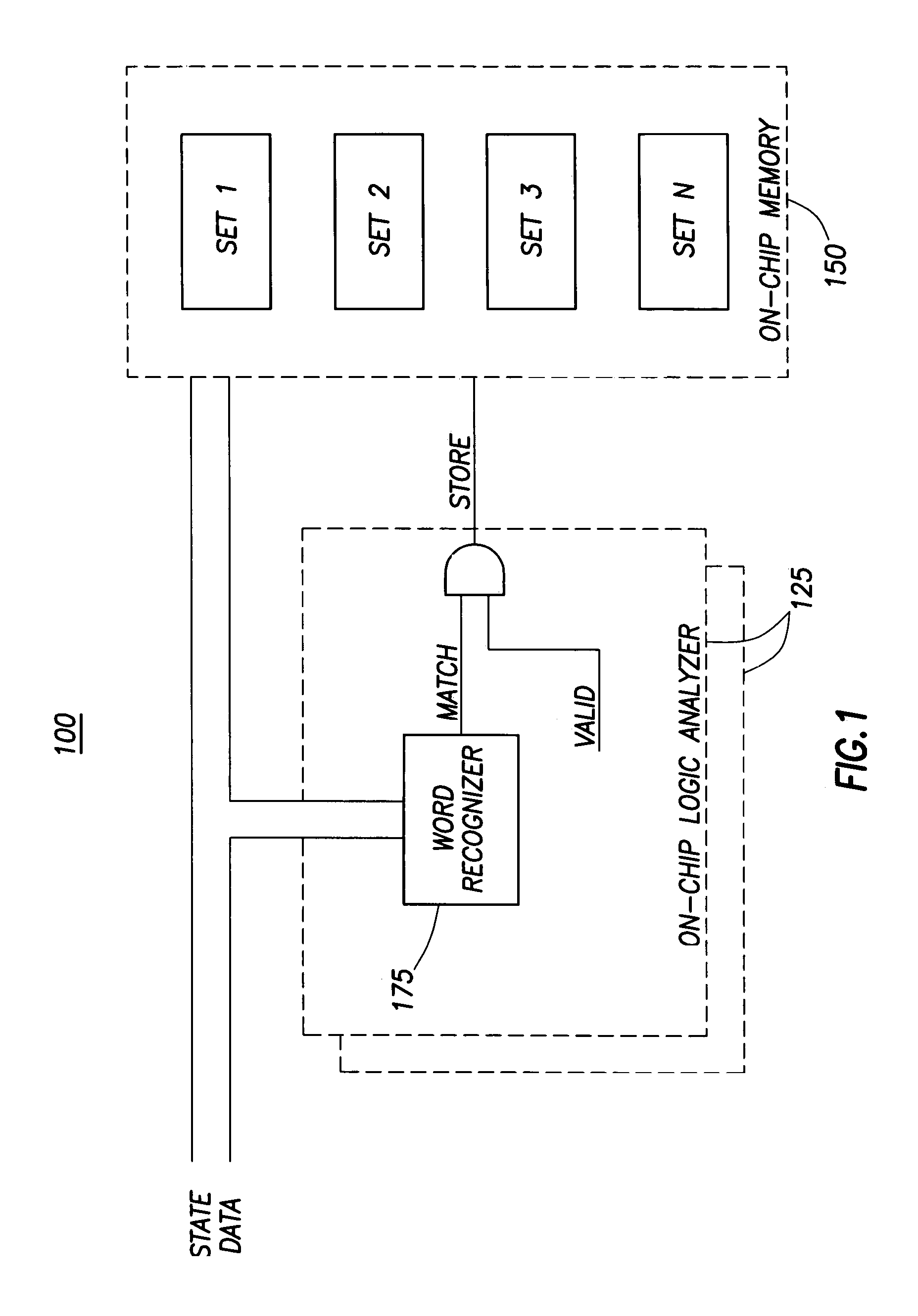
Consequently, if the OCLA stores all incoming internal state data in the cache, the cache would quickly overflow, and potentially relevant data would be overwritten, or ignored.
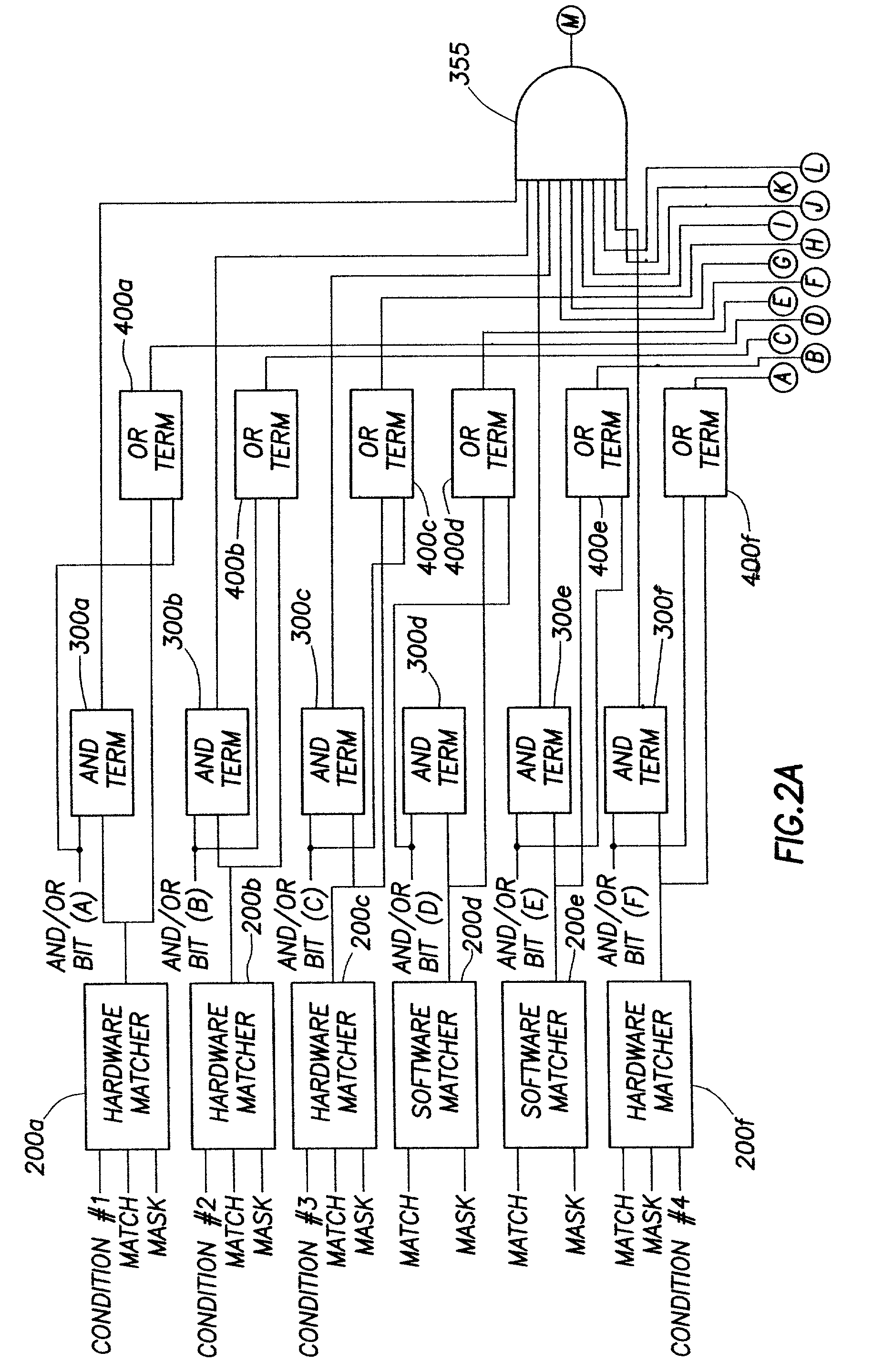
Unfortunately, implementing a full-feature word recognizer and associated counters and timers has been viewed as unfeasible on the chip itself because of the large number of wires, logic devices and processing time that such devices would require.
Thus, a full-feature word recognizer, capable of implementing arbitrary Boolean equations, typically is viewed as cost prohibitive to include on-chip.
The absence of a full-feature word recognizer in existing on-chip logic analyzers makes it much more difficult to debug a design, thus introducing additional time and money to the development of new processors and complex integrated circuits.
Despite the apparent advantages such a design would offer, to date no such product has developed.

Method used


Image

  • Efficient word recognizer for a logic analyzer
  • Efficient word recognizer for a logic analyzer
  • Efficient word recognizer for a logic analyzer

Examples


Embodiment Construction

[0038]Referring initially to FIG. 1, the present invention constructed in accordance with the preferred embodiment generally comprises an integrated circuit 100 that includes one or more on-chip logic analyzers 125 coupled to an on-chip memory device 150. In accordance with the preferred embodiment, the on-chip memory device 150 comprises an on-chip cache memory, and the integrated circuit comprises a processor. Various other devices may reside on the processor, including without limitation a memory controller (not shown) that controls accesses to a system memory (not shown), an I / O interface (not shown), and various other logical devices that interface with other components normally implemented in a computer system. In addition, the processor may be designed to operate in a multiple processor environment, and thus may include one or more interfaces for coupling to other processors in a computer system.

[0039]The cache memory 150 preferably comprises a cache memory located on-chip, a...


PUM


Abstract

A system having multiple on-chip logic analyzers (OCLA), each on-chip logic analyzer includes one or more word recognizers. The word recognizer includes a great deal of flexibility for the user, while being capable of implementation with very few gates. The word recognizer includes a Boolean logic portion in which a plurality of conditions can be dynamically segregated into a mutually exclusive set of groups. The conditions in each group are combined by means of a single Boolean function that is programmable. The resultant term (or product) from each group is combined with those of the other groups by a fixed selection of Boolean functions. The output of the Boolean logic section is provided to a counter / timer.

Description

CROSS-REFERENCE TO RELATED APPLICATIONS[0001]This application relates to the following commonly assigned co-pending applications entitled:[0002]Method And Apparatus For Efficiently Implementing Trace And / Or Logic Analysis Mechanisms On A Processor Chip, Ser. No. 10 / 034,717, filed Dec. 28, 2001 Method And Apparatus For Managing Timestamps When Storing Data, Ser. No. 10 / 034,462, filed Dec. 28, 2001; and Method And Apparatus For Implementing Loop Compression In A Program Counter Trace, Ser. No. 10 / 034,506, filed Dec. 28, 2001, now U.S. Pat. No. 6,691,207 issued Feb. 10, 2004.all of which are incorporated by reference herein.STATEMENT REGARDING FEDERALLY SPONSORED RESEARCH OR DEVELOPMENT[0003]Not applicable.BACKGROUND OF THE INVENTION[0004]1. Field of the Invention[0005]The present invention relates generally to logic analyzers that are used to facilitate the design of digital logic devices. More preferably, the present invention relates to an on-chip logic analyzer capable of receiving...

Claims


Application Information

Patent Timeline
Patent Type & Authority Patents(United States)
IPC IPC(8): G01R31/28G01R31/3177G06F11/25G06F11/273
CPCG01R31/3177G06F11/273G06F11/25
Inventor LITT, TIMOTHE
Owner HEWLETT PACKARD DEV CO LP
Why Eureka
Try Eureka