Plasma processing device
a processing device and plasma technology, applied in the direction of crystal growth process, chemically reactive gas, energy-based chemical/physical/physical-chemical process, etc., can solve the problems of insufficient plasma excitation efficiency, inconvenient use of shower plate, and inability to use gas of low decomposition temperature for plasma gas
- Summary
- Abstract
- Description
- Claims
- Application Information
AI Technical Summary
Benefits of technology
Problems solved by technology
Method used
Image

Examples
first embodiment
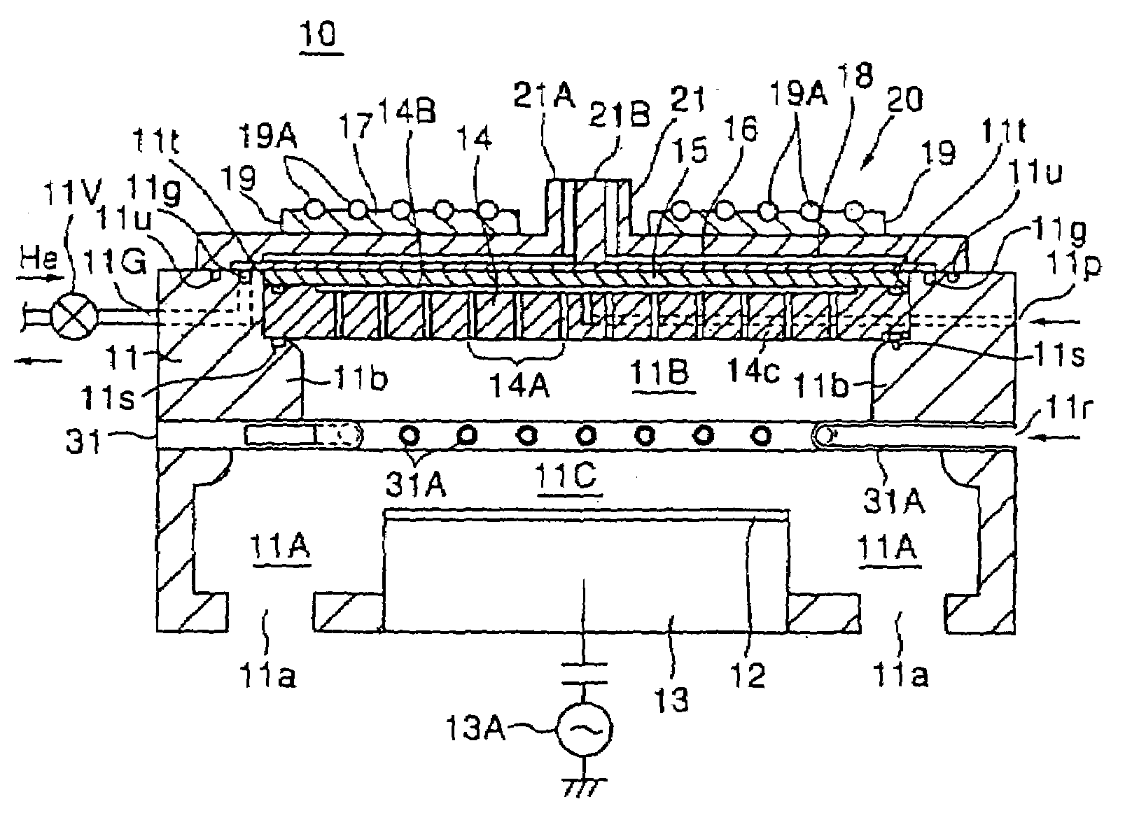
[0112]FIGS. 3A and 3B are diagrams showing the construction of a microwave plasma processing apparatus 10 according to a first embodiment of the present invention.
[0113]Referring to FIG. 3A, the microwave plasma processing apparatus 10 includes a processing vessel 11 and a stage 13 provided in the processing vessel 11 for holding a substrate 12 to be processed by an electrostatic chuck, wherein the stage 13 is preferably formed of AlN or Al2O3 by a hot isostatic pressing (HIP) process. In the processing vessel 11, there are formed two or three evacuation ports 11a in a space 11A surrounding the stage 13 with an equal distance, and hence with an axial symmetry with respect to the substrate 12 on the stage 13. The processing vessel 11 is evacuated to a low pressure via the evacuation port 11a by a gradational lead screw pump to be explained later.
[0114]The processing vessel 11 is preferably formed of an austenite stainless steel containing Al, and there is formed a protective film of ...
second embodiment
[0142]FIG. 10 shows the construction of a plasma processing apparatus 10A according to a second embodiment of the present invention, wherein those parts explained previously are designated by the same reference numerals and the description thereof will be omitted.
[0143]Referring to FIG. 2, the plasma processing apparatus 10A has a construction similar to the plasma processing apparatus 10 of FIGS. 3A and 3B except that the shower plate 14 is removed and a gas inlet port 11P extends into the space 11B in the processing vessel 11 from the gas inlet port 11p.
[0144]In such a construction, too, it is possible to form high-density plasma in the space 11B by exciting the plasma gas introduced from the gas inlet port 11P by the microwave supplied from the radial line slot antenna 20.
[0145]The high-density plasma thus formed may be somewhat inferior to the high-density plasma obtained for the case of using the shower plate 14 in terms of uniformity, but the plasma processing apparatus 10A h...
third embodiment
[0147]FIG. 11 is shows the construction of a microwave plasma processing apparatus 10B according to a second embodiment of the present invention, wherein those parts in FIG. 11 corresponding to the parts described previously are designated by the same reference numerals and the description thereof will be omitted.
[0148]Referring to FIG. 11, the microwave plasma processing apparatus 10B of the present embodiment has a construction similar to that of the microwave plasma processing apparatus 10 of the previous embodiment, except that the process gas supply structure 13 is removed in the microwave plasma processing apparatus 10B of the present embodiment. Further, the extension part 11b of the processing vessel 11 is formed with a round surface for avoiding electric discharge.
[0149]In the plasma processing apparatus 10B of such a construction, the plasma formed right underneath the shower plate 14 reflects the microwave, and thus, there occurs no problems such as the microwave reaching...
PUM
| Property | Measurement | Unit |
|---|---|---|
| Pressure | aaaaa | aaaaa |
| Pressure | aaaaa | aaaaa |
| Electrical conductor | aaaaa | aaaaa |
Abstract
Description
Claims
Application Information
 - R&D
- Intellectual Property
- Life Sciences
- Materials
- Tech Scout
- Unparalleled Data Quality
- Higher Quality Content
- 60% Fewer Hallucinations
Browse by: Latest US Patents, China's latest patents, Technical Efficacy Thesaurus, Application Domain, Technology Topic, Popular Technical Reports.
© 2025 PatSnap. All rights reserved.Legal|Privacy policy|Modern Slavery Act Transparency Statement|Sitemap|About US| Contact US: help@patsnap.com