
Trench capacitor and method for preparing the same

Active Publication Date: 2006-08-29
PROMOS TECH INC
View PDF5 Cites 0 Cited by
  • Summary
  • Abstract
  • Description
  • Claims
  • Application Information

AI Technical Summary

Benefits of technology

[0007]The objective of the present invention is to provide a trench capacitor for a dynamic random access memory and a method for preparing the same, which possesses a larger process window than the prior art, and can eliminate dangling bonds on an exposed surface of a semiconductor substrate.
[0010]Compared to the prior art using a shallow trench isolation to prevent the trench capacitors from being a short circuit, the present invention uses the first block of the collar oxide layer to isolate two adjacent capacitive structures so as to avoid the occurrence of the short circuit between the two adjacent capacitive structures. Using the first block as isolation also requires a smaller space. In addition, the etching process performed after the first block and the second block have been formed will not substantially etch the collar oxide layer. Consequently, there is a larger process window using the first block to isolate the two adjacent capacitive structures, and the trench capacitor can be used in a smaller fabrication generation. Furthermore, since the dangling bond on the exposed surface of the semiconductor substrate may reduce the mobility of carriers, the interface layer is formed on the exposed surface of the semiconductor substrate to eliminate dangling bonds according to the present invention.

Problems solved by technology

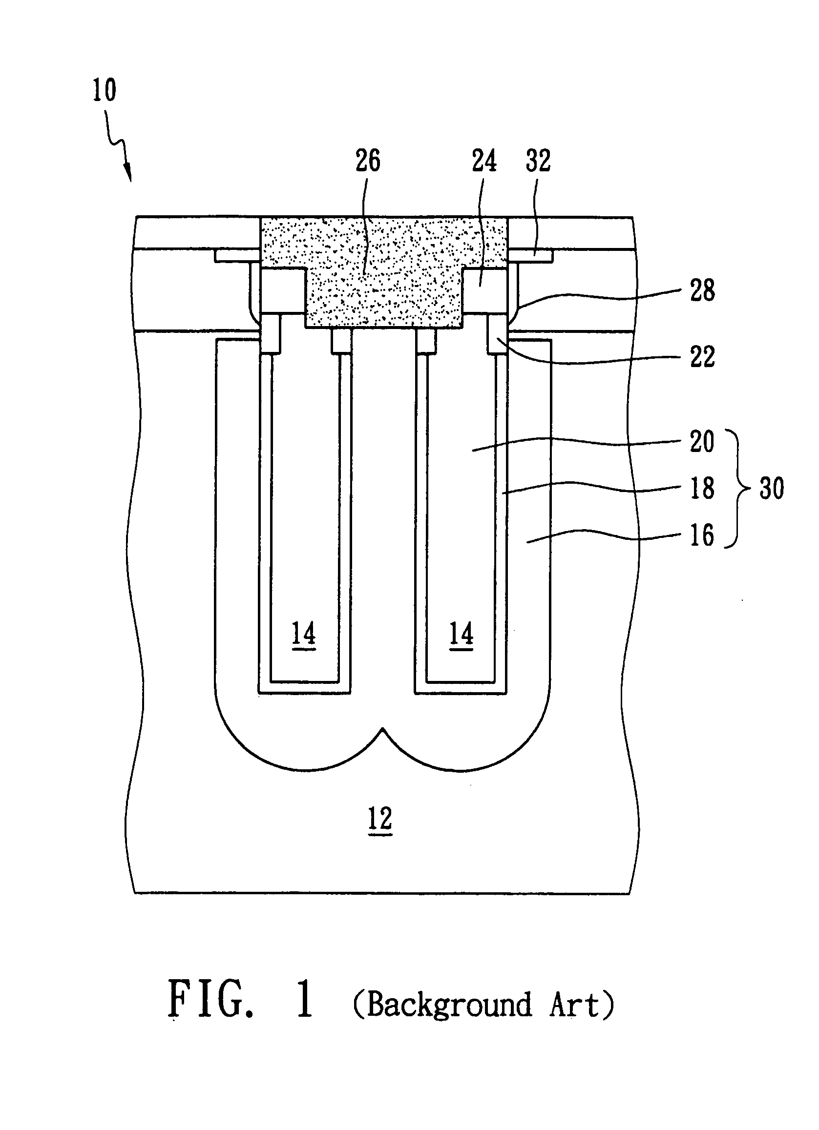
However, the lithographic process, which is used to define the position and the size of the shallow trench isolation 26, tends to generate misalignment as the size shrinks.
Consequently, the position of the shallow trench isolation 26 deviates from the predetermined position due to the misalignment of the lithographic process, which results in the occurrence of short circuit between the two capacitive structures 30.

Method used


Image

  • Trench capacitor and method for preparing the same
  • Trench capacitor and method for preparing the same
  • Trench capacitor and method for preparing the same

Examples


Embodiment Construction

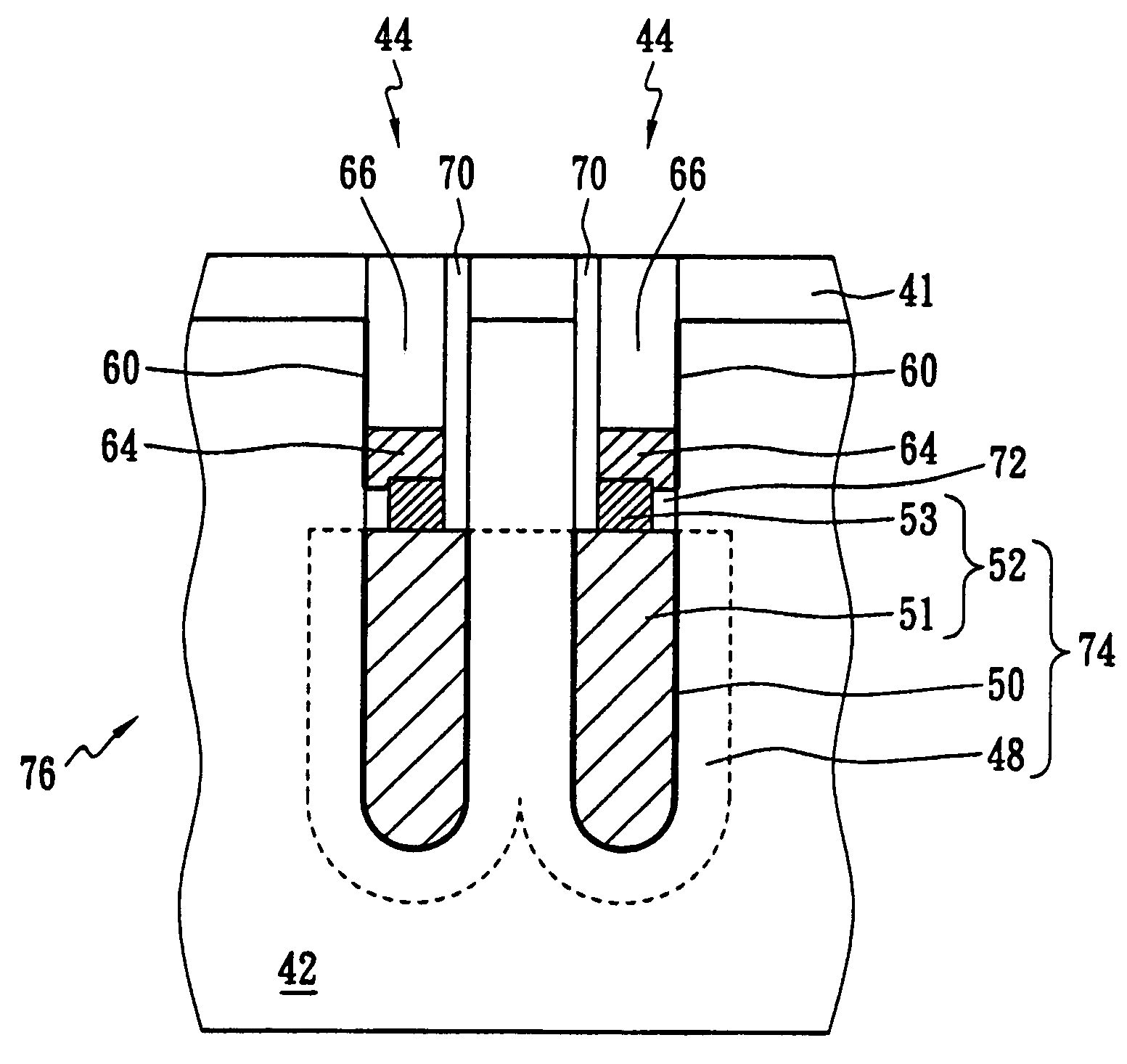
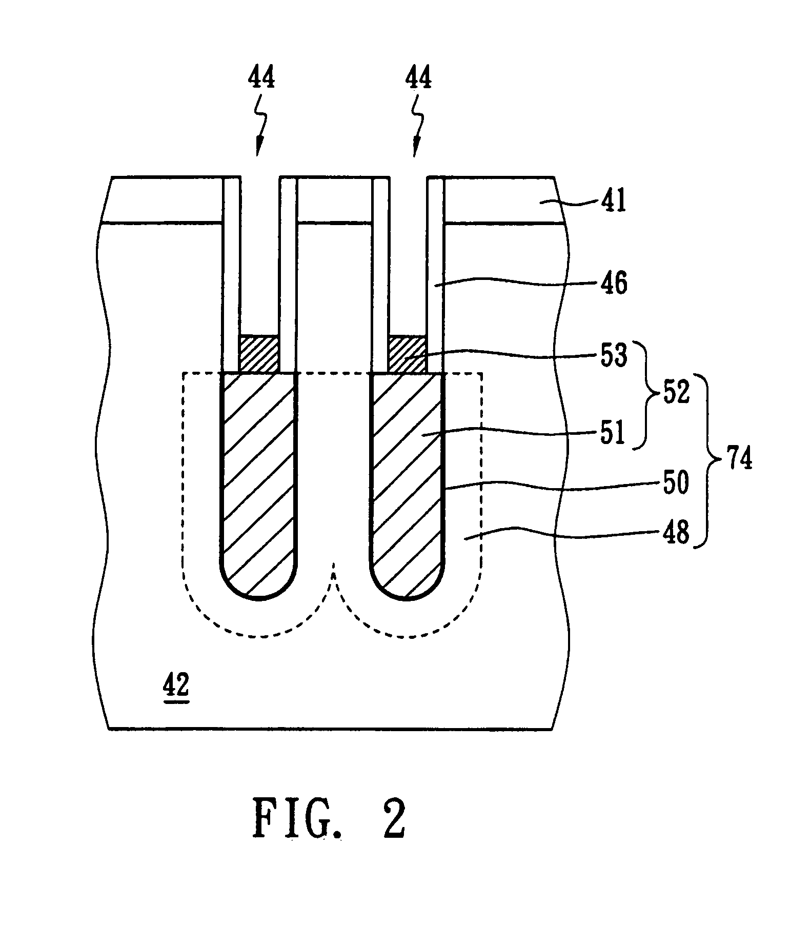
[0014]FIGS. 2 to 8 illustrate a method for preparing a trench capacitor 76 according to one preferred embodiment of the present invention. Referring to FIG. 2, after two adjacent trenches 44 are formed in a semiconductor substrate 42 with a silicon nitride layer 41 thereon, a bottom electrode 48 is formed on a lower outer surface of the trench 44, a dielectric layer 50 is formed on a lower inner surface of the trench 44, and a conductive layer 51 is formed on the dielectric layer 50 in sequences. A collar oxide layer 46 is then formed on an upper inner surface of the trench 44 by a thermal oxidation process (or chemical vapor deposition process) incorporating an anisotropic etching process. Another conductive layer 53 is formed on the conductive layer 51 to construct a top electrode 52. The bottom electrode 48, the dielectric layer 50 and the top electrode 52 form a capacitive structure 74.

[0015]Referring to FIGS. 3 and 4, a polysilicon layer 54 is formed on the semiconductor substr...


PUM


Abstract

The present invention discloses a trench capacitor formed in a trench in a semiconductor substrate. The trench capacitor comprises a bottom electrode positioned on a lower outer surface of the trench, a dielectric layer positioned on an inner surface of the bottom electrode, a top electrode positioned on the dielectric layer, a collar oxide layer positioned on an upper inner surface of the trench, a buried conductive strap positioned on the top electrode, and an interface layer made of silicon nitride positioned at the side of the buried conductive strap. The bottom electrode, the dielectric layer and the top electrode form a capacitive structure. The collar oxide layer includes a first block and a second block, and the height of the first block is larger than the height of the second block. The interface layer is positioned on a portion of the inner surface of the trench above the second block.

Description

BACKGROUND OF THE INVENTION[0001](A) Field of the Invention[0002]The present invention relates to a trench capacitor and a method for preparing the same, and more particularly, to a trench capacitor for a dynamic random access memory and a method for preparing the same.[0003](B) Description of the Related Art[0004]A memory cell of the dynamic random access memory (DRAM) includes an access transistor and a storage capacitor, wherein the source of the access transistor is electrically connected to a top electrode of the storage capacitor, and a bottom electrode of the storage capacitor is biased to a positive voltage. Particularly, the more the electric charges being stored in the storage capacitor, the less the occurrence of the error generated from the interpretation of data by a sensing amplifier due to the influence of noise. Therefore, current memory cells of the DRAM use 3-D capacitors, such as stacked capacitors or trench capacitors, to increase electric charges of the storage ...

Claims


Application Information

Patent Timeline
IPC IPC(8): H01L21/8234
CPCH01L29/66181H01L27/10861H10B12/038
Inventor LI, HUI MINCHIEN, JUNG WUCHUNG, CHAO HSILIN, MING HUNG
Owner PROMOS TECH INC
Learn More