Buck-boost circuit with normally off JFET

a buck-boost circuit and circuit technology, applied in the direction of power conversion systems, instruments, process and machine control, etc., can solve the problems of slow switching speed, limited frequency, certain amount of energy loss, etc., and achieve short switching transition times, small internal resistance, and small internal resistance

Inactive Publication Date: 2006-08-29
POWER INTEGRATIONS INC
View PDF10 Cites 23 Cited by
  • Summary
  • Abstract
  • Description
  • Claims
  • Application Information

AI Technical Summary

Benefits of technology

[0010]In one embodiment of the present invention, a buck-boost converter using a normally off JFET is constructed in the form of a two-port network. The negative input terminal is electrically connected to the negative output terminal to form a common ground. A dc power source is connected across the terminals of the input port. A normally off, or enhancement mode, n-channel JFET is used as a switching device with source connected to the positive input terminal and drain connected to an internal common node. Control circuitry within the two-port applies a switching control signal to the gate of the JFET. The internal circuit consists of a semiconductor diode, an inductor and a capacitor. The anode of the diode is connected to the positive output terminal and the cathode is connected to the internal common node. The inductor is connected between the internal common node and the common ground. The capacitor is connected across the output terminals. The JFET has very low terminal voltage source to drain when in the on or conducting state. That is to say, the JFET has a very small internal resistance between source and drain in the on state. The current carriers in the JFET are all majority carriers which results in very short switching transition times. As a result, this circuit offers significant improvements over existing circuits in high frequency switching as well as high power applications.
[0011]In a second embodiment, an n-channel enhancement mode and a p-channel enhancement mode JFET are used as switching devices in a buck-boost converter circuit. The circuit topology is the same as the first configuration with the diode replaced by the p-channel JFET. The p-channel JFET is connected with source to the positive output terminal and drain to the internal common node. The gates of the two JFETs are connected together, and a switching signal is applied to the gates by means of an internal control circuit. The switching signal alternately holds one JFET in the conducting state while the other JFET is simultaneously held in the current blocking state, and then switches each JFET to the opposite state. Both JFETs have a very low terminal voltage source to drain when in the on or conducting state. That is to say, each JFET has a very small internal resistance between source and drain in the on state. The current carriers in the JFETs are all majority carriers which results in very short switching transition times. As a result, this circuit also offers significant improvements over existing circuits in high frequency switching as well as high power applications.
[0012]For both the first and second configurations, the internal switching control circuitry can be realized with simple current control to vary both frequency and duty cycle. Furthermore, high frequency applications can be accomplished without the need for complex zero voltage switching, zero current switching or synchronous rectifying circuitry.

Problems solved by technology

Limits on both frequency of operation and duty cycle result from slow switching speeds.
Each time a device switches between states, a certain amount of energy is lost.
The slower the device switching time, the greater the power loss in the circuit.

Method used


Image

  • Buck-boost circuit with normally off JFET
  • Buck-boost circuit with normally off JFET
  • Buck-boost circuit with normally off JFET

Examples


Embodiment Construction

[0019]In the following detailed description of the present invention, a buck-boost circuit with normally off JFET, numerous specific details are set forth in order to provide a thorough understanding of the present invention. However, it will be obvious to one skilled in the art that the present invention may be practiced without these specific details. In other instances well known methods, procedures, components, and circuits have not been described in detail as not to unnecessarily obscure aspects of the present invention.

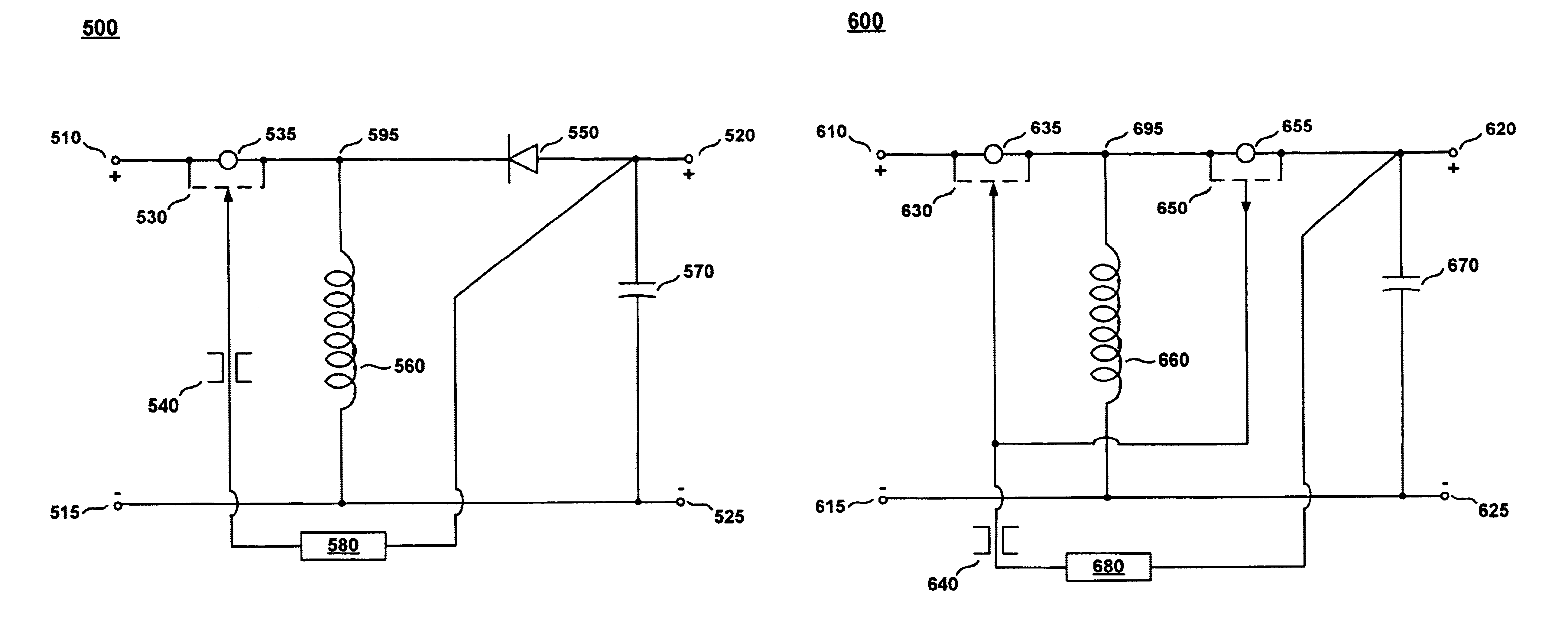
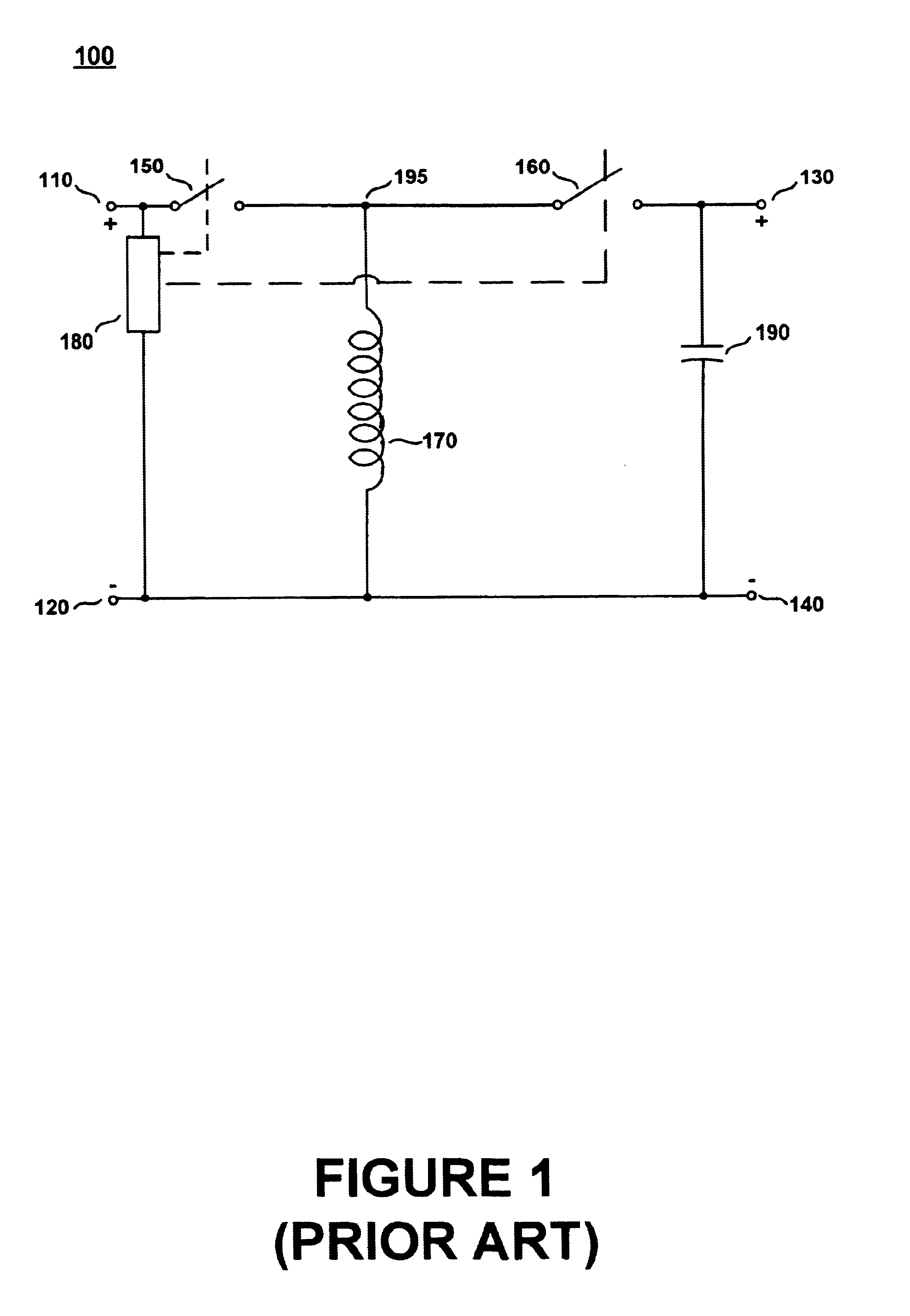
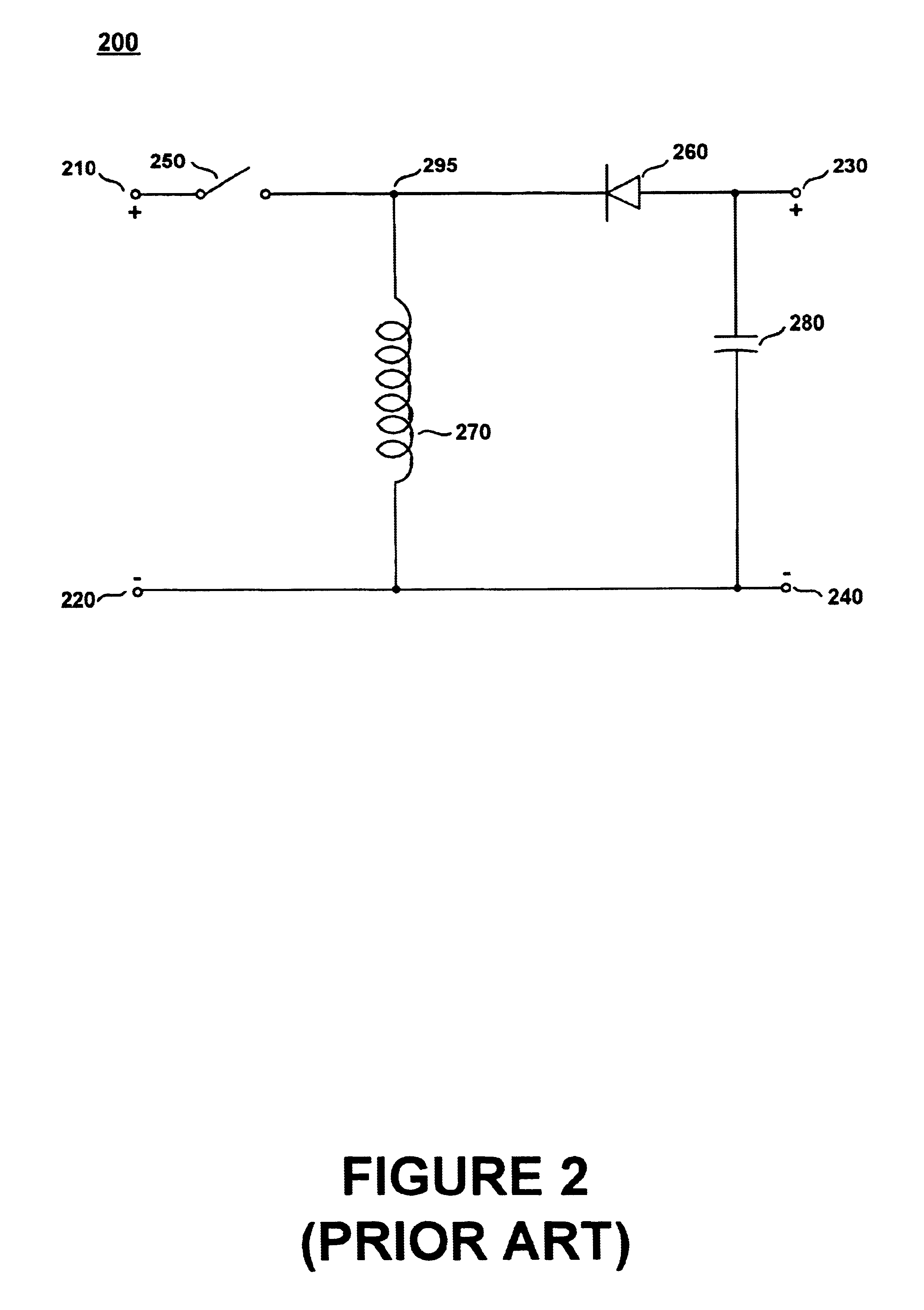
[0020]The generic diagram for a dc-dc buck-boost converter circuit 100 is shown in FIG. 1 as a two-port network having a positive input terminal 110, a positive output terminal 130, and a negative input terminal 120 connected to a negative output terminal 140. A capacitor 190 placed across the output terminals filters the dc output voltage and also acts as an electrical load. A first switch150 is connected between the positive input and an internal node 195. A s...


PUM


Abstract

An enhancement mode JFET as a switching device in a buck-boost converter circuit combined with a single rectifier diode and an inductor. A control circuit coupled to the gate of the JFET switches the JFET between a current conducting state and a current blocking state. The ratio of converter output voltage to converter input voltage is determined by the ratio of JFET current blocking time to the sum of JFET conduction time and JFET blocking time. This pulse width modulation scheme is thus used to adjust the dc output voltage level.

Description

[0001]The following copending U.S. patent application Ser. No. 09 / 430,500, “NOVEL JFET STRUCTURE AND MANUFACTURE METHOD FOR LOW ON RESISTANCE AND LOW VOLTAGE APPLICATIONS”, Ho-Yuan Yu, filed 29 Oct. 1999, is incorporated herein by reference for all purposes. The following U.S. provisional patent application Ser. No. 60 / 167,959, “STARTER DEVICE FOR NORMALLY “OFF” JFETS”, Ho-Yuan Yu, filed 29 Nov. 1999, is incorporated herein by reference for all purposes.BACKGROUND OF THE INVENTION[0002]Related ApplicationsFIELD OF THE INVENTION[0003]The present invention relates to the field of direct current (dc) power supplies designed for converting a given dc voltage to another dc voltage or dc current. More particularly, the present invention relates to utilization of enhancement mode Junction Field Effect Transistor (JFET) to construct dc-dD converters commonly known as buck-boost converters.RELATED ART[0004]Modem electronic circuit applications frequently require dc power supplied at several ...

Claims


Application Information

Patent Timeline
Patent Type & Authority Patents(United States)
IPC IPC(8): G05F1/613
CPCH02M1/08
Inventor YU, HO-YUAN
Owner POWER INTEGRATIONS INC
Why Eureka
Try Eureka