Methods for epitaxial silicon growth

Active Publication Date: 2006-09-05
MICRON TECH INC
View PDF10 Cites 3 Cited by
  • Summary
  • Abstract
  • Description
  • Claims
  • Application Information

AI Technical Summary

Benefits of technology

[0005]In accordance with an embodiment of the present invention, a method of cleaning a semiconductor surface is provided. The method comprises; providing a wafer, wherein the wafer has an upper surface, and wherein the wafer has a silicon area on the upper surface; forming a plasma from a gas flow, wherein the gas flow comprises an etchant gas; and exposing the upper surface of the wafer to the plasma. The exposure of the upper surface of the wafer to the plasma cleans the upper surface and renders the silicon area suitable for subsequent epitaxial silicon growth.
[0006]In accordance with another embodiment of the present invention, a method of growing epitaxial silicon is provided. The method comprises providing a wafer, wherein the wafer has an upper surface, and wherein the wafer has a silicon area on the upper surface. The method further comprises forming a RF plasma from a gas flow, wherein the gas flow comprises an etchant gas, and exposing the upper surface of the wafer to the RF plasma. The exposure of the upper surface of the wafer to the RF plasma renders the silicon area suitable for epitaxial silicon growth. The method also comprises growing epitaxial silicon on the silicon area subsequent to the exposure of the upper surface of the wafer to the RF plasma.
[0007]In accordance with yet another embodiment of the present invention, a method of growing epitaxial silicon is provided. The method comprises providing a wafer. The wafer has an upper surface, and the wafer has a first silicon area on the upper surface. Additionally, the wafer has a first dielectric area on the upper surface. The method further comprises forming a RF plasma from a gas flow, wherein the gas flow comprises at least one etchant gas. The method comprises exposing the upper surface of the wafer to the RF plasma. The exposure of the upper surface of the wafer to the RF plasma renders the first silicon area suitable for epitaxial silicon growth. The method also comprises growing epitaxial silicon on the first silicon area subsequent to the exposure of the u

Problems solved by technology

However, epitaxial silicon growth on silicon areas cleaned in this manner may exhibit a high degree of unwanted lateral growth.
Additionally, dielectric layers that are subsequently exposed to epitaxial sili

Method used


Image

  • Methods for epitaxial silicon growth
  • Methods for epitaxial silicon growth
  • Methods for epitaxial silicon growth

Examples


example 1

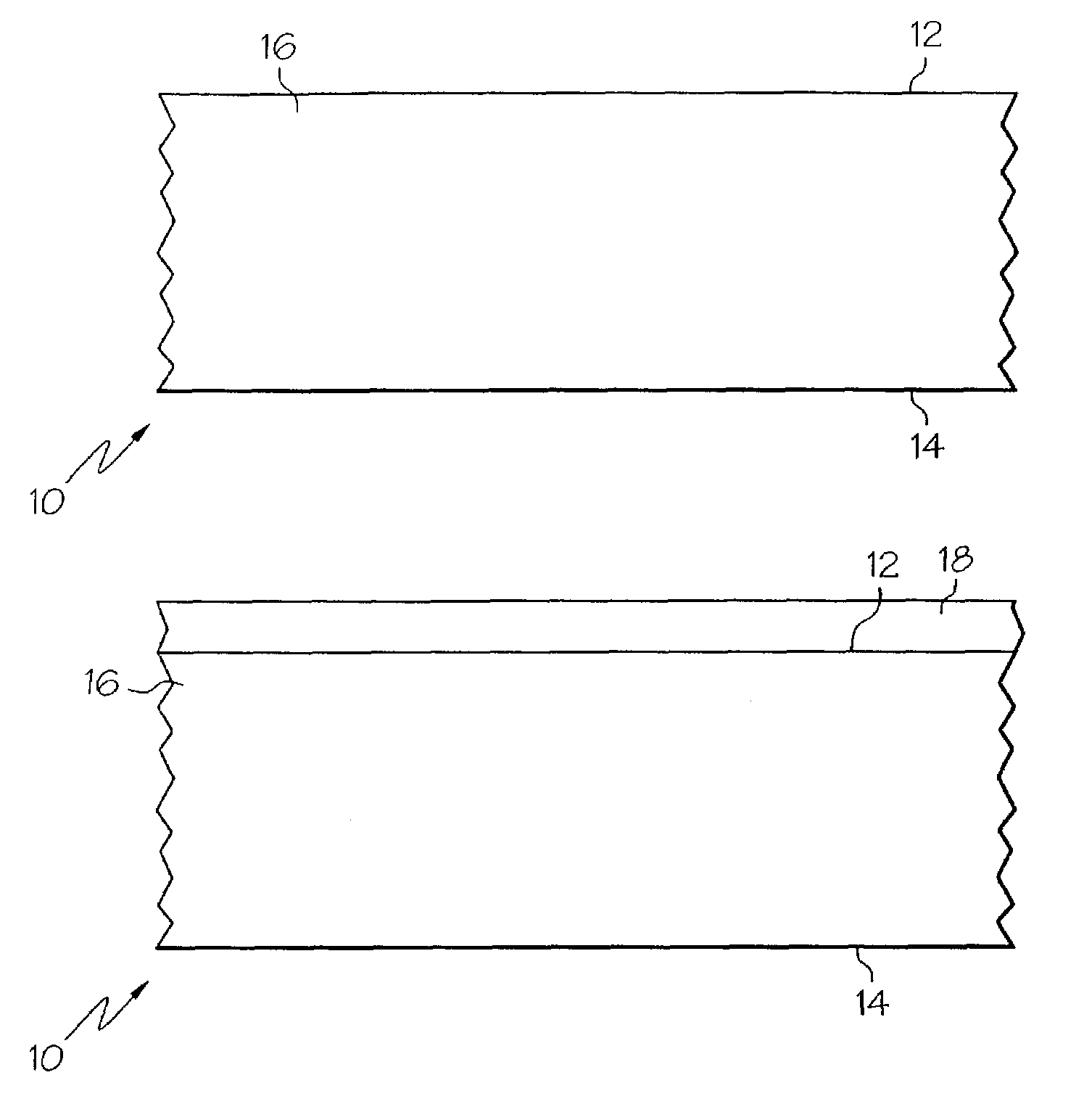
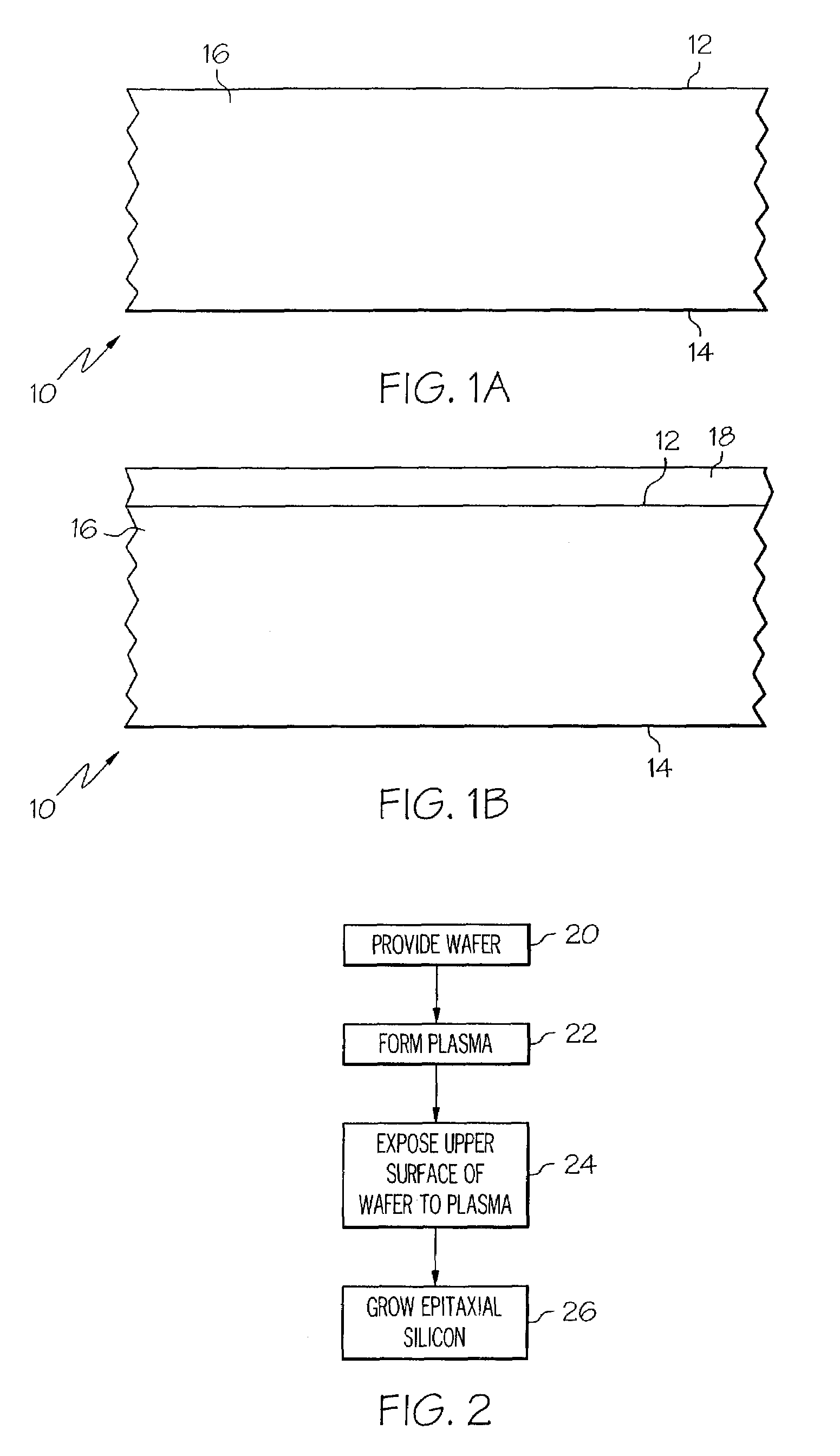
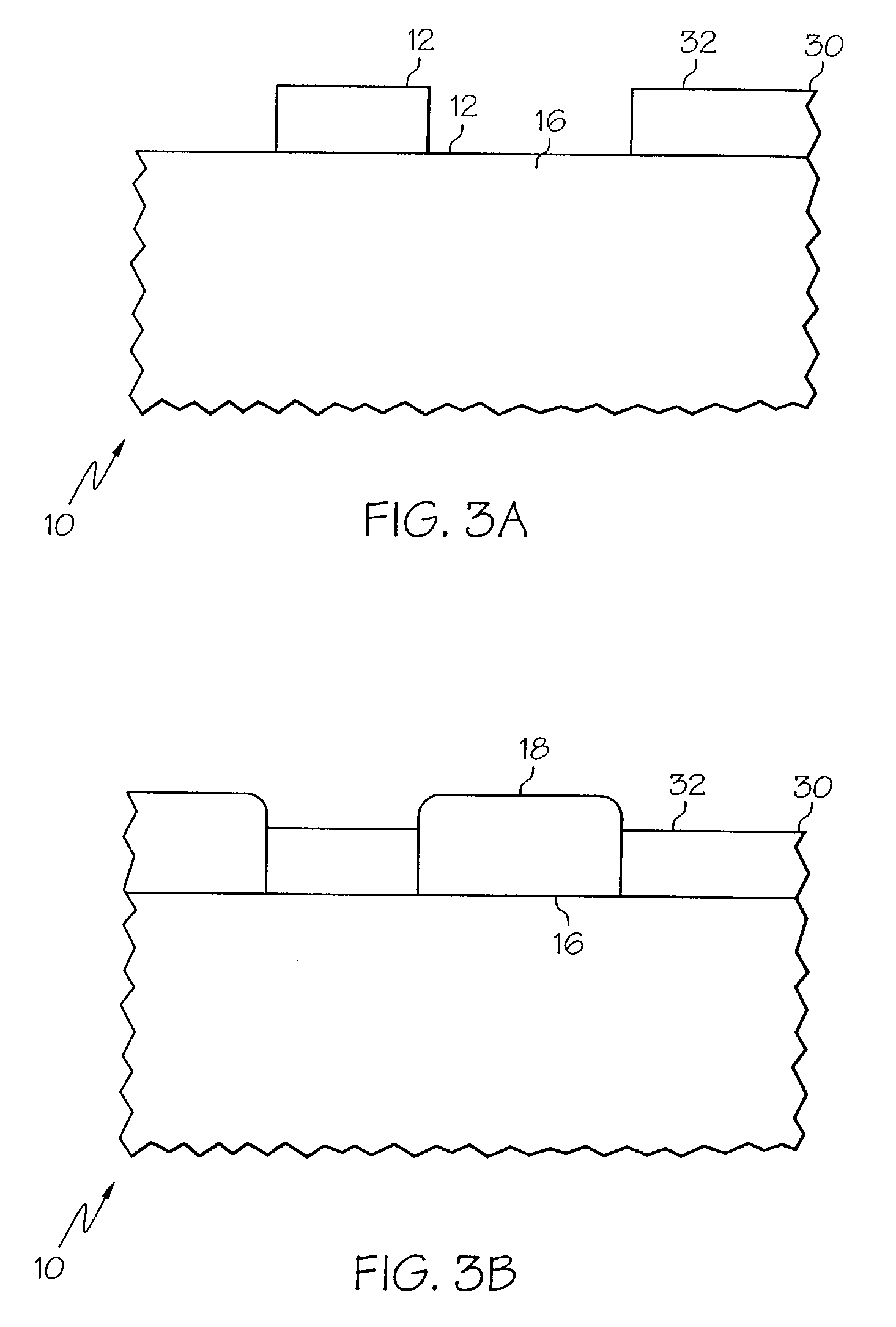
[0026]A wafer having silicon areas and silicon nitride areas on an upper surface was exposed to a RF plasma formed from an SF6 gas flow flowing at 40 sccm. The RF power was 300 W, and the wafer was exposed to the plasma for 60 seconds.

[0027]Epitaxial silicon was subsequently grown on the silicon areas. The epitaxial silicon was grown by a SiH6, Cl2, and H2 gas flow present with a 10−8 Torr background pressure. The growth was continued for between about 5 to about 25 minutes in order to achieve a desired thickness of epitaxial silicon. The nitride areas did not exhibit significant epitaxial silicon growth, and it was apparent that the RF plasma had passivated the surface of the nitride.

example 2

[0028]A wafer having polysilicon areas and silicon nitride areas on an upper surface was exposed to a RF plasma formed from an SF6 gas flow flowing at 40 sccm. The RF power was 300 W, and the wafer was exposed to the plasma for 60 seconds.

[0029]Epitaxial polysilicon was subsequently grown on the silicon areas. The epitaxial silicon was grown by a SiH6, Cl2, and H2 gas flow present with a 10−8 Torr background pressure. The growth was continued for between about 5 to about 25 minutes in order to achieve a desired thickness of epitaxial polysilicon. The nitride areas did not exhibit significant epitaxial polysilicon growth, and it was apparent that the RF plasma had passivated the surface of the nitride.

example 3

[0030]A wafer having silicon areas and silicon oxide areas on an upper surface was exposed to a RF plasma for 60 seconds. The plasma was formed from a 40 sccm gas flow of SF6, and the RF power was 300 W.

[0031]Epitaxial silicon was grown on the silicon areas by a SiH6, Cl2, and H2 gas flow present with a 10−8 Torr background pressure. The growth was continued for between about 5 to about 25 minutes in order to achieve a desired thickness of epitaxial silicon. The epitaxial silicon exhibited a lateral growth rate to vertical growth rate ratio of about 1:4, as measured by comparing the height of the vertical growth to the width of the lateral growth.


PUM


Abstract

Methods of cleaning substrates and growing epitaxial silicon thereon are provided. Wafers are exposed to a plasma for a sufficient time prior to epitaxial silicon growth, in order to clean the wafers. The methods exhibit enhanced selectivity and reduced lateral growth of epitaxial silicon. The wafers may have dielectric areas that are passivated by the exposure of the wafer to a plasma.

Description

BACKGROUND OF THE INVENTION[0001]Epitaxial silicon is used in a variety of semiconductor devices when a pure silicon layer is required. Epitaxial silicon is generally grown on a substrate and exhibits the same crystal structure as the substrate on which it is grown. Epitaxial silicon layers may have their doping type or concentration controlled independently from the substrate on which the layers are grown. Generally, the substrate on which epitaxial silicon is to be grown must be cleaned prior to the growth to remove impurities and ensure that the epitaxial silicon layer is of a high quality.[0002]One approach to cleaning substrates prior to epitaxial silicon growth is to wash the substrate using hydrofluoric acid and to subsequently hydrogen bake the substrate at high temperatures. However, epitaxial silicon growth on silicon areas cleaned in this manner may exhibit a high degree of unwanted lateral growth. Additionally, dielectric layers that are subsequently exposed to epitaxial...

Claims


Application Information

Patent Timeline
IPC IPC(8): C30B25/16C30B23/02C30B25/02C30B25/18
CPCC30B23/02C30B29/06C30B25/18
Inventor ZHANG, JINGYANPING, ER-XUAN
Owner MICRON TECH INC
Why Eureka
Try Eureka