
Semiconductor device including first and second transistor groups and semiconductor integrated circuit device

a semiconductor integrated circuit and semiconductor technology, applied in semiconductor devices, semiconductor/solid-state device details, electrical apparatus, etc., can solve the problems of complicated structure and complicate layout design, and achieve excellent electrostatic discharge (esd) resistance, suppress the increase in gate delay time, and facilitate layout design

Inactive Publication Date: 2006-09-05
LAPIS SEMICON CO LTD
View PDF4 Cites 2 Cited by
  • Summary
  • Abstract
  • Description
  • Claims
  • Application Information

AI Technical Summary

Benefits of technology

[0029]An object of the present invention is to provide a semiconductor device and a semiconductor integrated circuit device, which can solve the above described problem, which excellently accomplish a high-speed device and low power consumption, which are less likely to cause ESD damage, and which can reduce a gate resistance and make a layout design relatively easy.
[0033]According to the invention, a semiconductor device, which has excellent electrostatic discharge (ESD) resistance, which suppresses a gate resistance, thereby suppressing increase in a gate delay time, which facilitates layout design and has no risk of damage on an oxide film under a gate electrode, is provided. Further, a semiconductor integrated circuit device employing the semiconductor device in an output circuit thereof is provided.

Problems solved by technology

Therefore, the structure becomes complicated and this complicates the layout design.

Method used


Image

  • Semiconductor device including first and second transistor groups and semiconductor integrated circuit device
  • Semiconductor device including first and second transistor groups and semiconductor integrated circuit device
  • Semiconductor device including first and second transistor groups and semiconductor integrated circuit device

Examples


first embodiment

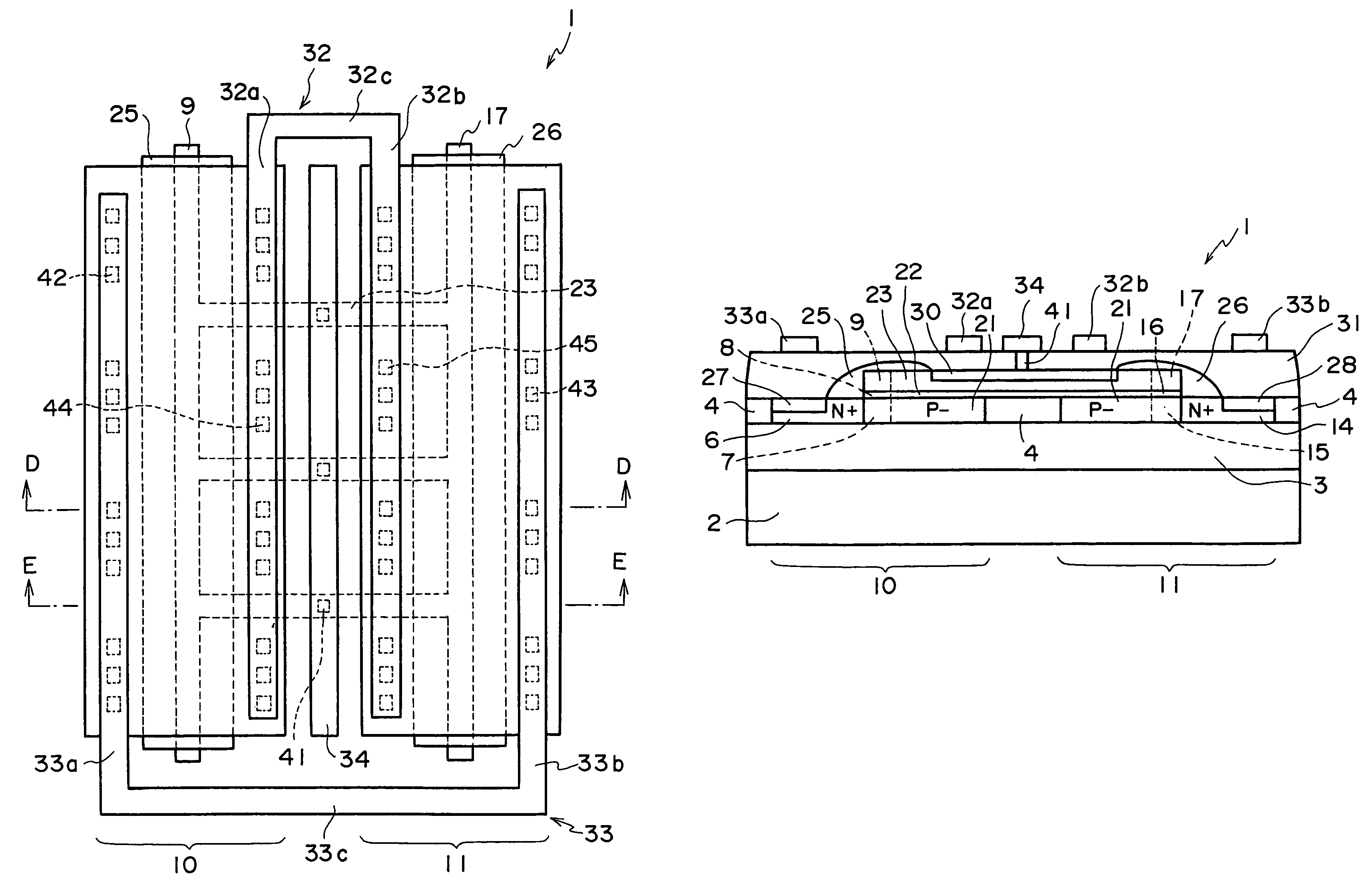
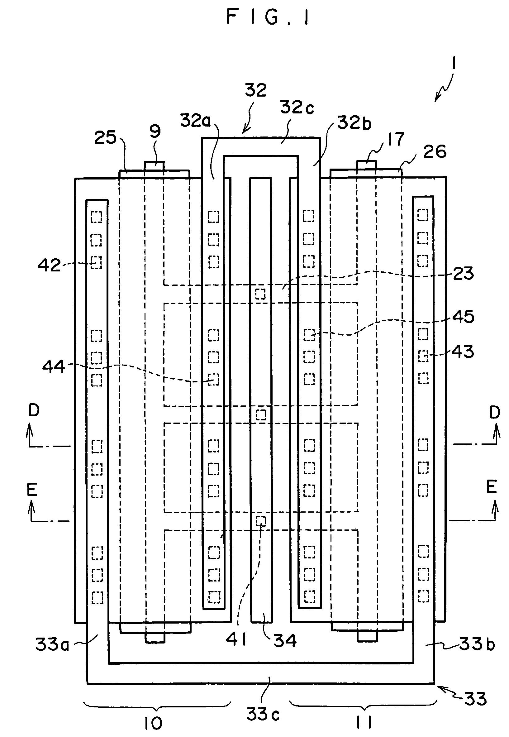
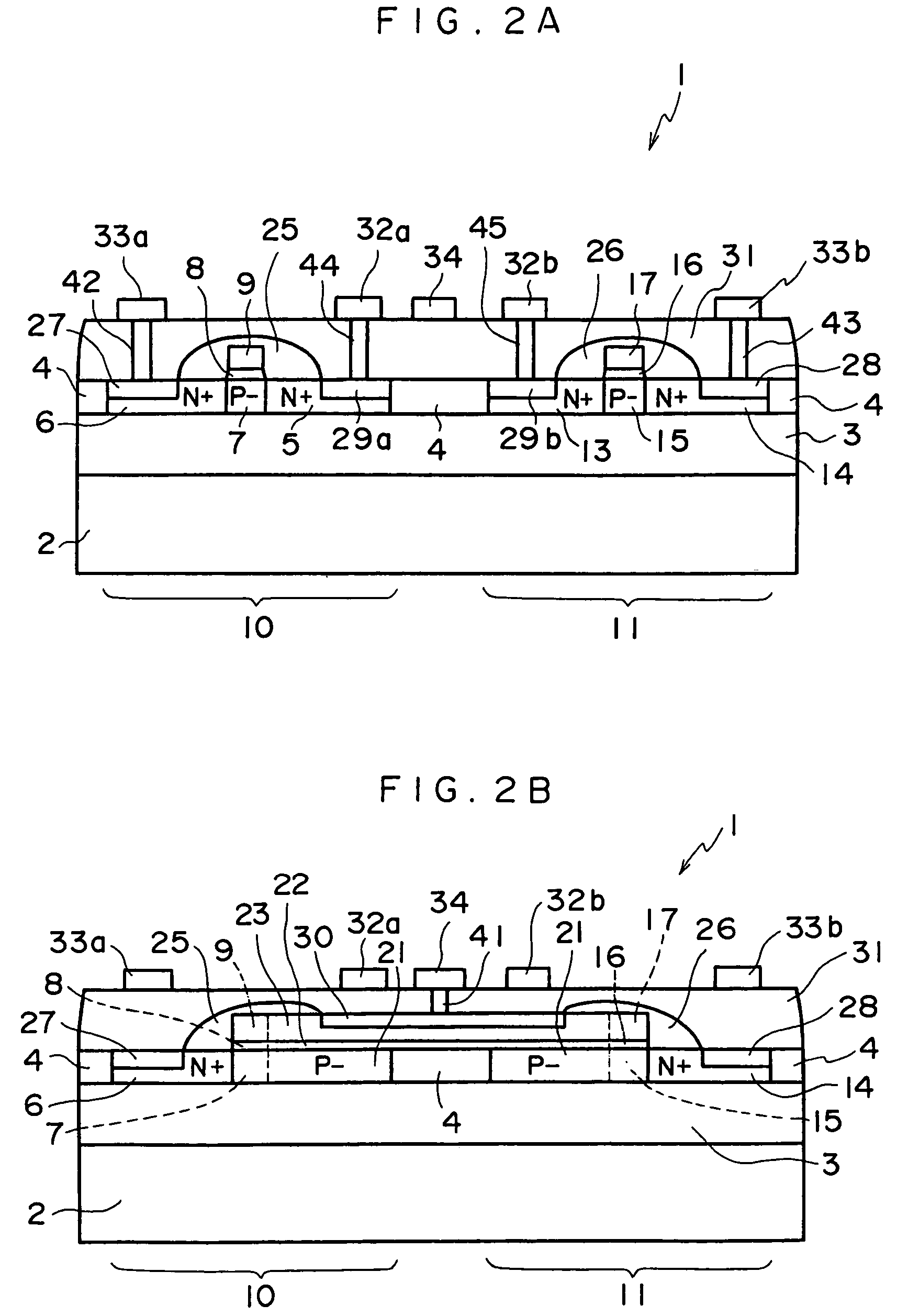
[0048]FIG. 1 is a plan view showing a salicide block NMOS transistor 1 forming a semiconductor device according to a first embodiment of the invention, FIG. 2A is a sectional view taken along line D—D in FIG. 1, and FIG. 2B is a sectional view taken along line E—E in FIG. 1.

[0049]As shown in these drawings, this semiconductor device includes a semiconductor substrate such as a P silicon substrate 2, a buried oxide film 3 formed on the substrate 2, and two thin silicon layers 10 and 11 formed on the oxide film 3, which are isolated from each other by a field oxide layer 4 serving as an element isolation layer.

[0050]In the example shown, the thin silicon layers 10 and 11 forming active regions are respectively formed in a longitudinally (in FIG. 1) elongated rectangular shape, and are arranged in parallel with and adjacent to each other.

[0051]In the thin silicon layer 10, a first N+ diffusion region 5 and a second N+ diffusion region 6 are formed by impurity diffusion, and a longitudi...

second embodiment

[0073]FIG. 3 is a plan view showing a structure of a salicide block NMOS transistor 51 forming a semiconductor device according to a second embodiment of the invention, FIG. 4A is a sectional view taken along line F—F in FIG. 3, and FIG. 4B is a sectional view taken along line G—G in FIG. 3. In the following description of the salicide block NMOS transistor 51 according to the second embodiment, elements which are common with those of the above-described salicide block NMOS transistor 1 of the first embodiment are designated by the same reference numerals and are not described in detail. Only differences between the first and the second embodiments are described in detail.

[0074]Main differences between the salicide block NMOS transistor 51 of the second embodiment and the above-described salicide block NMOS transistor 1 of the first embodiment shown in FIG. 1 lie in that no field oxide film layer 4 (see FIGS. 2A and 2B) for element isolation is provided, and a wiring portion 54 made...

third embodiment

[0090]FIG. 9 is a sectional view showing a structure of a salicide block NMOS transistor 71 according to a third embodiment based on the semiconductor device of the invention.

[0091]The salicide block NMOS transistor 71 is formed of two NMOS transistors, which are formed by a MOS process on a bulk substrate including a P-well 73 formed on a P-semiconductor substrate 72, in parallel with each other and isolated by element isolation oxide films 74, 75 and 76. This salicide block NMOS transistor 71 is equivalent to the above-described salicide block NMOS transistor 1 shown in FIGS. 1, 2A and 2B, where the SOI substrate of the salicide block NMOS transistor 1 is replaced with the bulk substrate.

[0092]Therefore, elements of the salicide block NMOS transistor 71 which are common with those of the salicide block NMOS transistor 1 of the first embodiment are designated by the same reference numerals or not shown in the drawings and are not described in detail. Only differences between the fi...


PUM


Abstract

A salicide block area is provided around a gate electrode. Polysilicon coupling portions are formed, which extend at plurality of points from the gate electrode to an area outside of an active region. A contact provided at this inactive region electrically connects the gate electrode to gate electrode metal wiring, which is provided above the gate electrode.

Description

CROSS-REFERENCE TO RELATED APPLICATION[0001]This application claims priority under 35 USC 119 from Japanese Patent Application No. 2003-311430, the disclosure of which is incorporated by reference herein.BACKGROUND OF THE INVENTION[0002]1. Field of the Invention[0003]The present invention relates to a semiconductor device and a semiconductor integrated circuit device. More particularly, the invention relates to a structure of a semiconductor device adapted for preventing electrostatic discharge damage, which is to be formed as an output circuit of a semiconductor integrated circuit device.[0004]2. Description of the Related Art[0005]An example of semiconductor devices, which are conventionally known as the above type of semiconductor device, includes: a gate electrode formed, via a gate insulating layer, on a semiconductor layer of a silicon substrate; an impurity diffused layer formed on a semiconductor layer of an active region and forming a source region or a drain region; and co...

Claims


Application Information

Patent Timeline
Patent Type & Authority Patents(United States)
IPC IPC(8): H01L23/62H01L21/28H01L21/3205H01L21/8234H01L21/84H01L23/52H01L27/088H01L27/12H01L29/423H01L29/49H01L29/78H01L29/786
CPCH01L27/1203H01L21/84
Inventor ICHIKAWA, KENJI
Owner LAPIS SEMICON CO LTD
Learn More