
High-frequency line-waveguide converter having the HF line terminated within an opening portion

Inactive Publication Date: 2006-09-05
KYOCERA CORP
View PDF9 Cites 12 Cited by
  • Summary
  • Abstract
  • Description
  • Claims
  • Application Information

AI Technical Summary

Benefits of technology

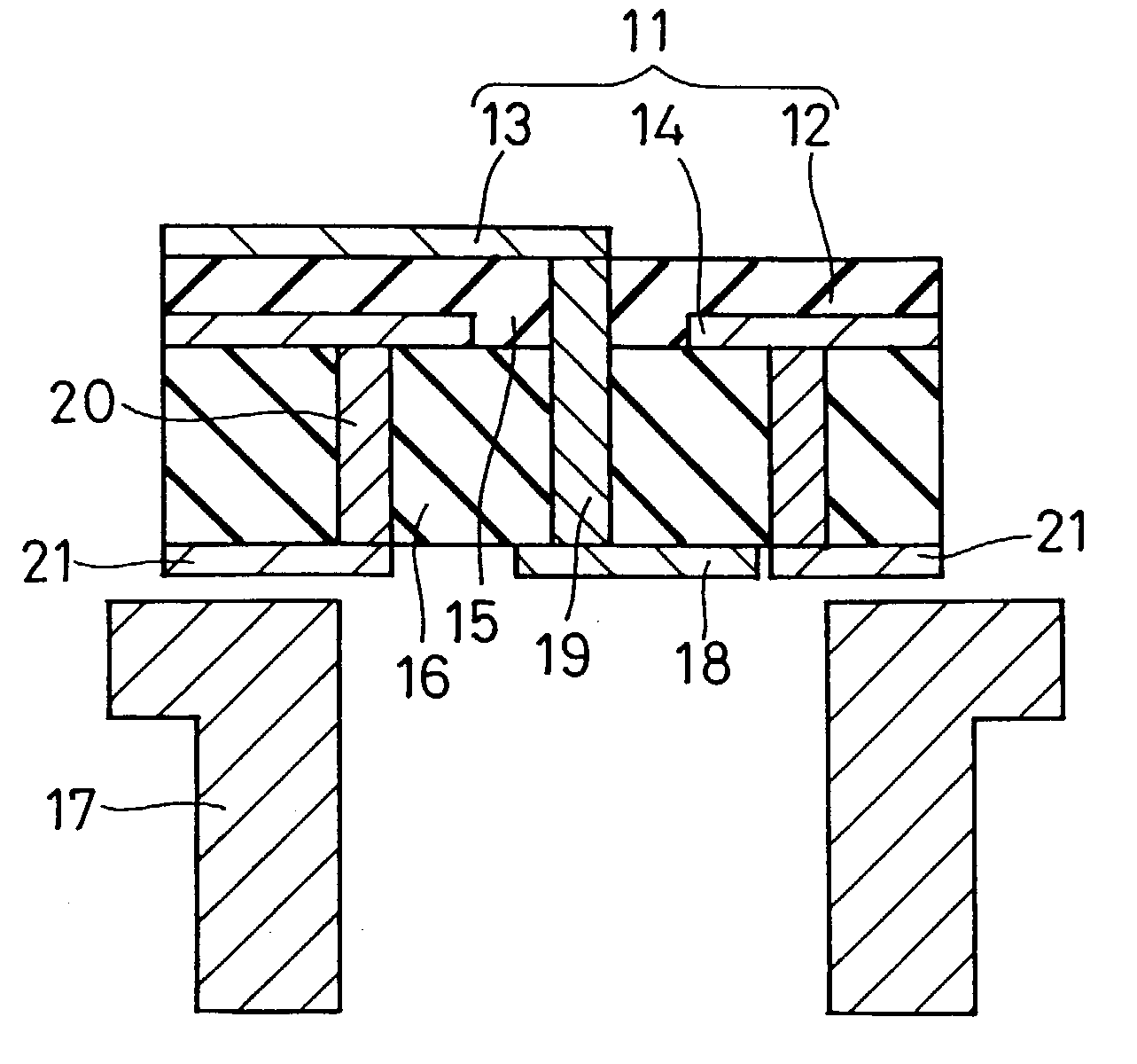
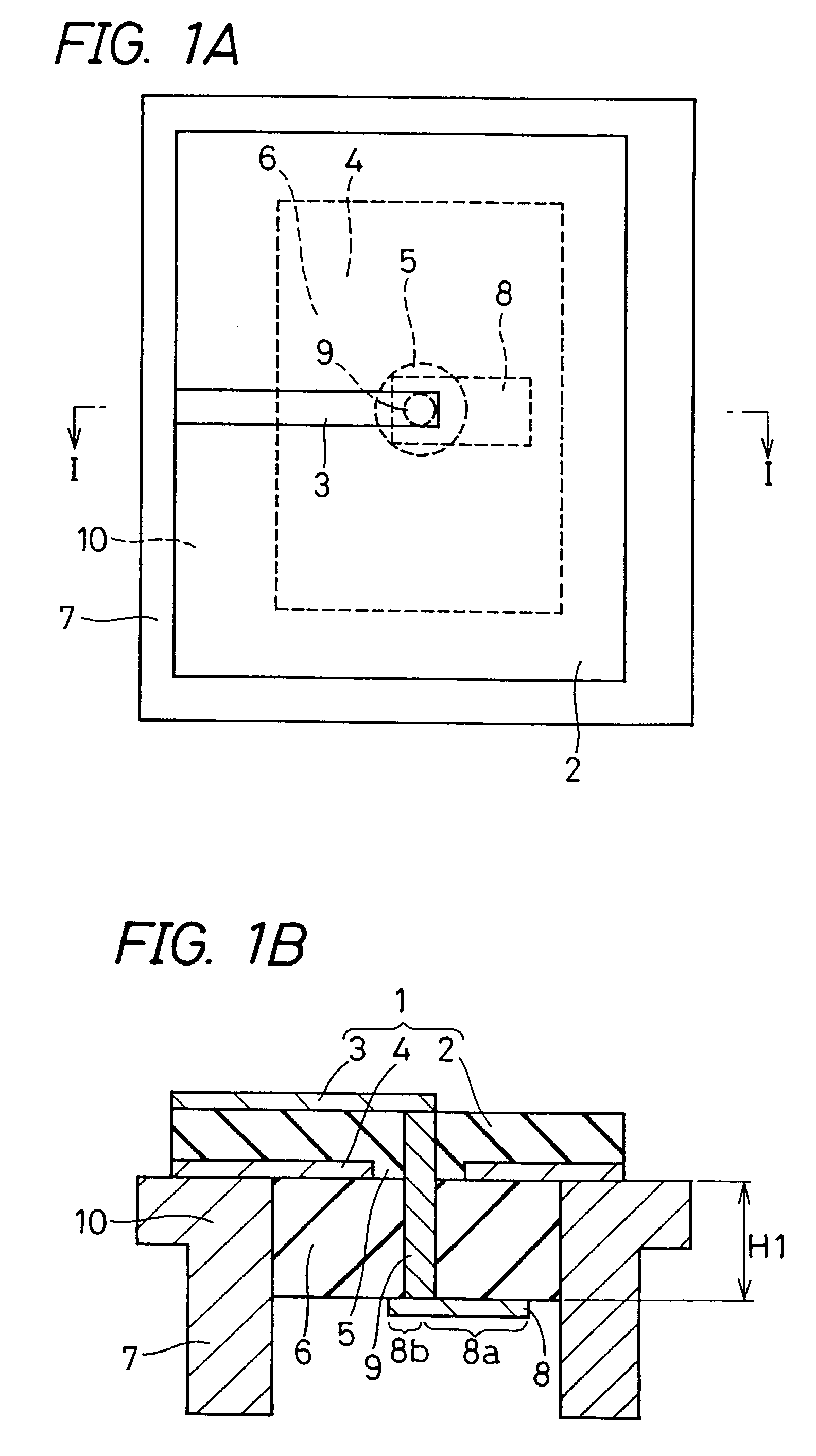
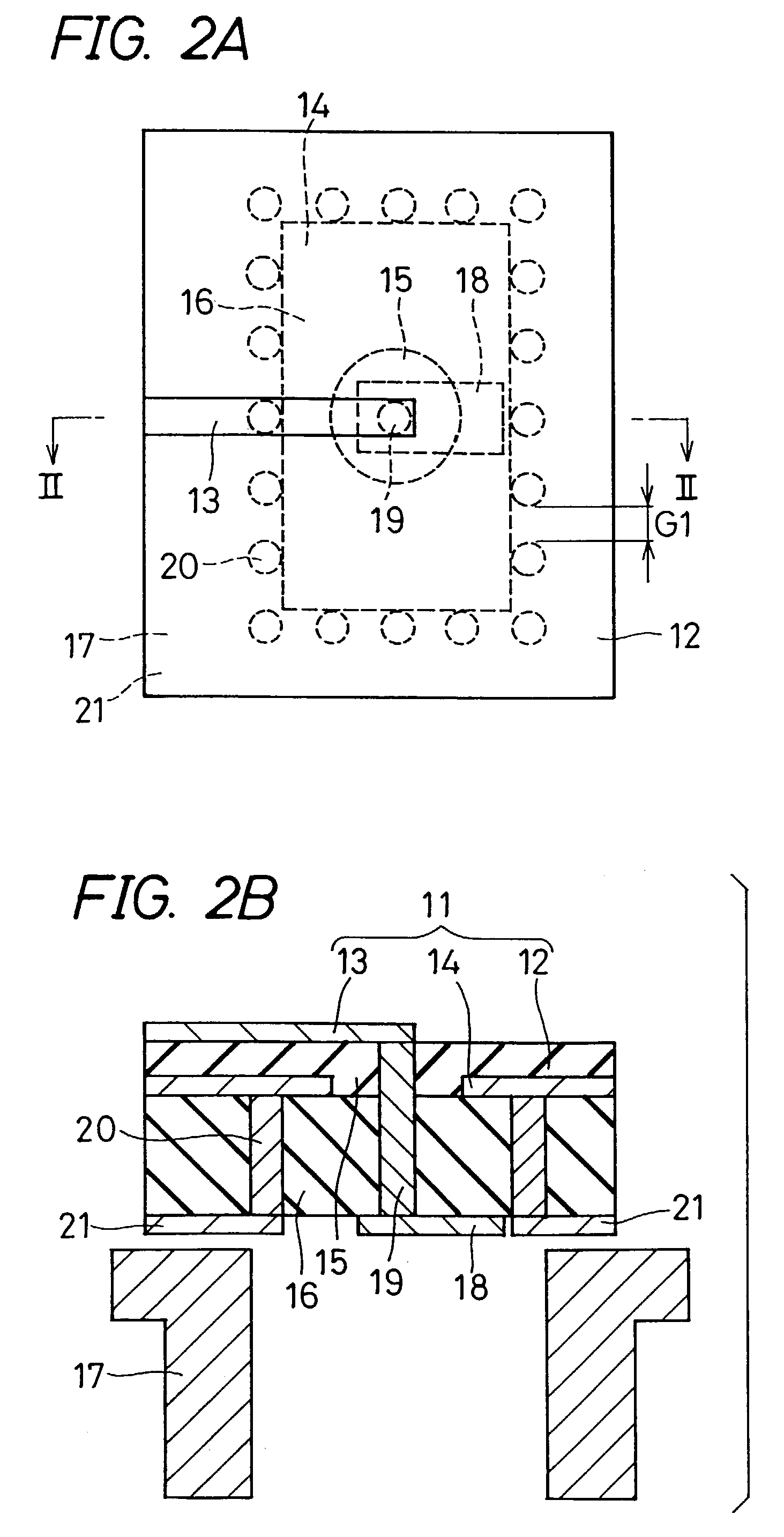
[0022]The invention has been devised in view of the above-described problems with the conventional art, and accordingly its one object is to provide a high-frequency line-waveguide converter in which a distance between grounding and radiating conductors is so determined that high-frequency line-waveguide conversion efficiency is enhanced; a thickness of a dielectric layer can be set freely for proper impedance adjustment to the high-frequency line; and no extra processing is required in an opening of the waveguide.
[0023]Another object of the invention is to provide a high-frequency line-waveguide converter which provides high conversion efficiency but incurs less variation in conversion characteristics.

Problems solved by technology

However, such a high-frequency system poses the following problem.
To compensate for these losses, it is necessary to make heavy use of expensive high-frequency components that are lower in noise but higher in efficiency and gain, resulting in the system as a whole being expensive.
Further, since the current flows through a relatively wide area in the tubular wall of the waveguide, the resultant electrical resistance decreases, resulting in the conductor loss being reduced.
Therefore, when the high-frequency line-waveguide converter incurs a significant conversion loss due to positional deviation of each component, all of the constituent components become useless.
This gives rise to a problem of the assembly yield being low.
However, this construction poses the following problems.
Consequently, depending on signal frequencies, a difference in conductor width is caused between the line conductor and its counterpart line conductor of the micro-strip line that are connected to each other, resulting in occurrence of signal reflection.
In this case, depending on materials used for the substrate, there is a possibility that the dielectric substrate is deformed or broken.
Thus, if the waveguide-planer line converter undergoes positional deviation and this causes a change in the length of the part functioning as an antenna, the antenna characteristics are varied, resulting in degradation of the conversion efficiency of the waveguide-planer line converter.
Thus, an electromagnetic wave leaks from this concavity, resulting in degradation of the conversion efficiency.
This gives rise to a problem of the conversion characteristics being varied easily.
This makes it difficult to stabilize the characteristics by conducting an examination.

Method used


Image

  • High-frequency line-waveguide converter having the HF line terminated within an opening portion
  • High-frequency line-waveguide converter having the HF line terminated within an opening portion
  • High-frequency line-waveguide converter having the HF line terminated within an opening portion

Examples


example

[0140]Next, the following experiments are conducted to confirm the effect exerted by the high-frequency line-waveguide converter embodying the invention.

[0141]At first, using an alumina-ceramics green sheet whose dielectric loss tangent is 0.0006 at 10 GHz after firing and a metallized paste for tungsten metallization, an evaluative substrate as shown in FIGS. 8A to 8C is fabricated by means of ordinary green-sheet laminating technique and simultaneous firing technique. Note that FIG. 8A is a top view of the evaluative substrate; FIG. 8B is a sectional view taken on the line VIII—VIII of FIG. 8A; and FIG. 8C is a bottom view.

[0142]After firing, nickel and gold plating is applied to the surfaces of the metallized layers formed on the top and bottom surfaces, respectively, of the evaluative substrate. Here, the high-frequency line-waveguide converter incorporated in the evaluative substrate is so designed that its corresponding waveguide is of a WR-10 waveguide for use in the W-band (...


PUM


Abstract

An object of the invention is to provide a high-frequency line-waveguide converter in which a distance between a grounding conductor and a radiating conductor and a thickness of a dielectric layer of a high-frequency line can be freely set. A high-frequency line-waveguide converter for converting a high-frequency line to a waveguide comprises a high-frequency line including a first dielectric layer; a line conductor; and a grounding conductor; an opening portion of the grounding conductor; a second dielectric layer; a radiating conductor; a connecting conductor; a shielding conductor portion; and a waveguide.

Description

BACKGROUND OF THE INVENTION[0001]1. Field of the Invention[0002]The present invention relates to a high-frequency line-waveguide converter for converting a high-frequency line which is used in a microwave or millimeter wave band and constitutes a high-frequency circuit (such as a strip line, a microstrip line, a coplanar line, or a coplanar line having a grounding conductor) to a waveguide, the high-frequency line-waveguide converter having succeeded in facilitating system mounting by providing connection between a high-frequency circuit and an antenna, or between high-frequency circuits, through a waveguide.[0003]2. Description of the Related Art[0004]In recent years, as we move into the so-called advanced information age, signals in an increasingly wider range of frequencies have been sought after for information transmission. Consequently, studies have been conducted as to the use of signals falling in a range from micro-wave-band frequencies (1 to 30 GHz) to millimeter-wave-band...

Claims


Application Information

Patent Timeline
IPC IPC(8): H01P5/107
CPCH01L23/66H01P5/107H01L2924/01068H01L2224/48091H01L2224/48137H01L2924/01012H01L2924/0102H01L2924/01078H01L2924/01079H01L2924/09701H01L2924/16195H01L2924/19039H01L2924/3011H01L2924/3025H01L2223/6633H01L24/48H01L2924/00014H01L2924/00015H01L24/45H01L2224/85399H01L2224/05599H01L2224/45099H01L2224/45015H01L2924/207
Inventor KORIYAMA, SHINICHIUCHIMURA, HIROSHI
Owner KYOCERA CORP
Learn More