Methods for estimating the body voltage of digital partially depleted silicon-on-insulator circuits

a technology of silicon-on-insulator circuit and body voltage, which is applied in the field of parts depleted silicon-on-insulator technology, can solve the problems of noise failure, floating body effect in pd-soi has posed and continues to pose major challenges, and fully-depleted devices have been largely abandoned in favor of partially-depleted technology, etc., and achieve accurate estimation of upper and lower bounds of body voltage.

Inactive Publication Date: 2006-09-05
THE TRUSTEES OF COLUMBIA UNIV IN THE CITY OF NEW YORK
View PDF8 Cites 34 Cited by
  • Summary
  • Abstract
  • Description
  • Claims
  • Application Information

AI Technical Summary

Benefits of technology

[0010]An object of the present invention is to provide a technique for accurately...

Problems solved by technology

For digital applications, fully-depleted devices have been largely abandoned in favor of partially-depleted technology, because of the difficulty in controlling the threshold voltage of fully-depleted thin-film transistors.
At the device and circuit level, however, the floating body effect in PD-SOI has posed and continues to pose major challenges in the successful use of this technology.
As discussed in Pong-Fei Lu et al., “Floating-body Effects in Partially Depleted SOI CMOS circuits, 32 IEEE J. Solid-State Circuits 1241 (1997), there is a parasitic bipolar effect which can result in noise failures if not correctly considered.
In addition, there can be large “uncertainties” in the body potential, and consequently the threshold voltage, of devices due to unknown past switching activity.
In addition, for many circuit styles in which noise margin is strongly deter...

Method used


Image

  • Methods for estimating the body voltage of digital partially depleted silicon-on-insulator circuits
  • Methods for estimating the body voltage of digital partially depleted silicon-on-insulator circuits
  • Methods for estimating the body voltage of digital partially depleted silicon-on-insulator circuits

Examples


case 1

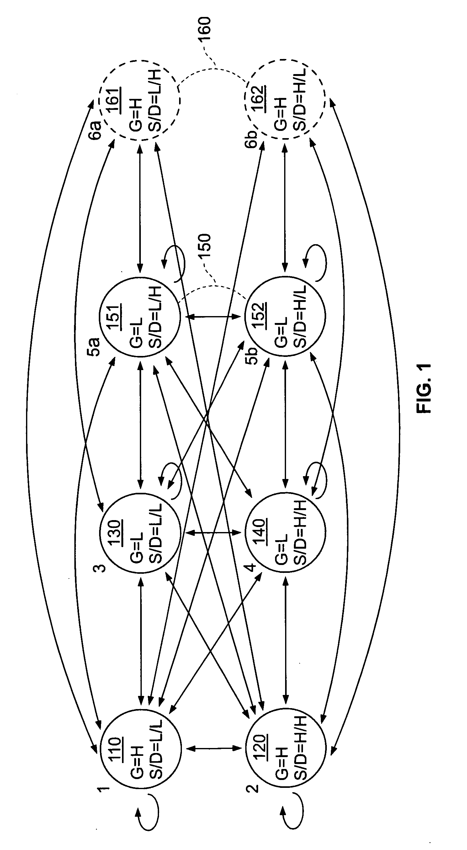
[0137]In Case 1, transistor M13 charges the internal node between transistors M1 and M2 to VDD every precharge phase. This configuration would be common in bulk CMOS to mitigate charge-sharing noise but is potentially disastrous for SOI since it can allow the body of M1 to easily charge to a very high bias, nearly 1 V. When brought into state 150 by the noise condition, M1 draws bipolar leakage current. The high body voltage also reduces the threshold voltage, making the FET more sensitive to the coupling noise on the gate.

case 3

[0138 is similar, but the fact that net E is under steady switching means that both states 120 and 140 are accessible for FET M5. State 2 accessibility limits the maximum body voltage possible to only about 0.75 V. In this case, the body voltage is not high enough to result in significant parasitic bipolar leakage but the threshold voltage is still reduced enough to result in functional failure.

[0139]In Case 2, transistor M14 discharges the internal node between transistors M3 and M4 every cycle. From the point of view of the modified accessibility analysis, this is equivalent to Case 4, in which both E and F are active. The conservative upper bound overestimates the body voltage. The main reason for this discrepancy is the neglect of state 160 which is exerting a downward pressure on the body voltage which is not (in the interests of conservatism) considered in the modified accessibility analysis.


PUM


Abstract

Techniques for estimating a body voltage of one or more transistors which form digital partially depleted silicon-on-insulator circuit, and for using estimated voltages to analyze electrical properties of the circuit, are disclosed. In one technique, device models are obtained and abstracted to generate simplified electrical descriptions of the transistors. The circuit topology is checked to generate sets of accessible states for the transistors that are indicative of whether a connection between a source or a drain of a transistor and either a power supply or ground exists. Next, sets of reference state body voltage minima and reference state body voltage maxima are determined for each of the transistors based on corresponding simplified electrical descriptions and corresponding sets of accessible states. Finally, a target state body voltage minima and a target state body voltage maxima are ascertained, one for each transistor, based on the determined sets of reference state body voltage minima and reference state body voltage maxima.

Description

[0001]This application claims priority to U.S. Provisional Application No. 60 / 138,842 filed on Jun. 10, 1999.NOTICE OF GOVERNMENT RIGHTS[0002]The U.S. Government has certain rights in this invention pursuant to the terms of the National Science Foundation award number CCR-97-34216.BACKGROUND OF THE INVENTION[0003]I. Field of the Invention[0004]The present invention relates to partially depleted silicon-on-insulator technology, and more particularly to techniques for estimating the body voltage of digital integrated circuits and partially depleted silicon-on-insulator (“PD-SOI”) technology.[0005]II. Description of the Related Art[0006]Silicon-on-insulator (“SOI”) technology has long been used for radiation-hardened or high-voltage integrated circuits. In more recent years, SOI has also been considered for us as a technology for high-performance, low-power deep-submicron digital integrated circuits. For digital applications, fully-depleted devices have been largely abandoned in favor ...

Claims


Application Information

Patent Timeline
IPC IPC(8): G06F17/50
CPCG06F17/5036G06F30/367
Inventor SHEPARD, KENNETH
Owner THE TRUSTEES OF COLUMBIA UNIV IN THE CITY OF NEW YORK
Why Eureka
Try Eureka