Method for calculation of cell delay time and method for layout optimization of semiconductor integrated circuit

a technology of integrated circuits and delay times, applied in the field of calculation of cell delay times and layout optimization of semiconductor integrated circuits, can solve the problems of different delay calculations, poor delay calculation accuracy, and design flow backward, and achieve the effects of low accuracy, low delay calculation accuracy, and high accuracy

Inactive Publication Date: 2006-09-12
SOCIONEXT INC
View PDF8 Cites 20 Cited by
  • Summary
  • Abstract
  • Description
  • Claims
  • Application Information

AI Technical Summary

Benefits of technology

[0053]In the cell delay time calculation method of the present invention, the dependence of an output signal waveform of a cell upon the input slew rate and cell load capacitance of the cell, i.e., a parameter showing signal waveform propagation dependence between the cell input and output terminals, is calculated. Then, based on the dependence thus calculated, it is determined which one of the delay calculation methods (i.e., the method that deals with signal waveform propagation between the cell input and output terminals and the method that does not deal with signal waveform propagation between the cell input and output terminals) is suitable for delay calculation. Then, according to the cell input slew rate and the load capacitance connected to the cell output terminal, a delay calculation tool with a high-accuracy delay calculation algorithm mounted therein is used for a portion that requires severe consideration for signal waveform propagation so as to calculate delay time at high accuracy. On the other hand, for a portion that does not require severe consideration for signal waveform propagation, a high-speed delay calculation tool, which is inferior in accuracy to the foregoing delay calculation tool, is used. Accordingly, the present invention is able to provide a high-speed and high-accuracy delay calculation method for delay calculation of an entire LSI circuit.
[0054]Further, in the semiconductor integrated circuit layout optimization method of the present invention, the dependency of the output signal waveform of a cell upon the input slew rate and load capacitance of the cell is calculated. If the dependence of a cell exceeds a predetermined dependence level, then the cell is subjected to re-layout so that the cell dependence becomes lower than the predetermined dependence level. This makes it possible to calculate delay times at high accuracy by using only a delay calculation tool having an algorithm that does not deal with signal waveform propagation between the cell input and output terminals.

Problems solved by technology

However, when performing a timing driven layout in the layout step S1300, if a delay calculation algorithm different from one used in the delay calculation step S1302 is employed, this causes these two steps to produce different delay calculation results.
For this reason, the problem with a layout by the timing driven layout is that the design flow is returned back to a particular design step due to the fact that different delay calculation algorithms produce different delay calculation results.
However, even when both the delay calculation tool and the layout tool employ the same delay calculation algorithm, if the layout step S1300 generates a layout shape that does not allow the delay calculation algorithm to perform delay calculations at high accuracy, this results in poor delay calculation accuracy.
However, such a measure has not yet been taken so far.
However, the first delay calculation method has some problems (FIG. 15).
This results in poor delay calculation accuracy.
One of the demerits is that the accuracy of delay calculations is poor for circuits with wires whose resistance and capacitance undergo considerable variation, as shown in FIG. 15(a).
Since, in addition to the delay calculation processing, it is required to determine a signal propagation sequence and to propagate information necessary for delay calculations according to the determined signal propagation sequence, this will take extra delay calculation processing time.
This produces the problem that there may be generated a layout form causing delay calculation difficulties to the delay calculation algorithm.
As a result, the delay calculation accuracy for such a layout becomes poor, which causes the design procedure to return back to a particular design step.
Further, the delay calculation method of FIG. 14 suffers the problem that the accuracy of delay calculation for a circuit having a configuration with wires whose resistance and capacitance undergo considerable variation becomes poor.
On the other hand, the delay calculation method of FIG. 16 also suffers the problem that it is required to perform path retrieval in the signal propagation direction.
This results in an increased length of delay calculation processing time.
However, most of the presently-used design flows employ only one of the delay calculation methods of FIGS. 14 and 16 and fail to make good utilization of both of them in effective manner.
In addition, in the conventional techniques there exists no index for effectively and properly using these two delay calculation methods during the layout stage.

Method used


Image

  • Method for calculation of cell delay time and method for layout optimization of semiconductor integrated circuit
  • Method for calculation of cell delay time and method for layout optimization of semiconductor integrated circuit
  • Method for calculation of cell delay time and method for layout optimization of semiconductor integrated circuit

Examples


embodiment 1

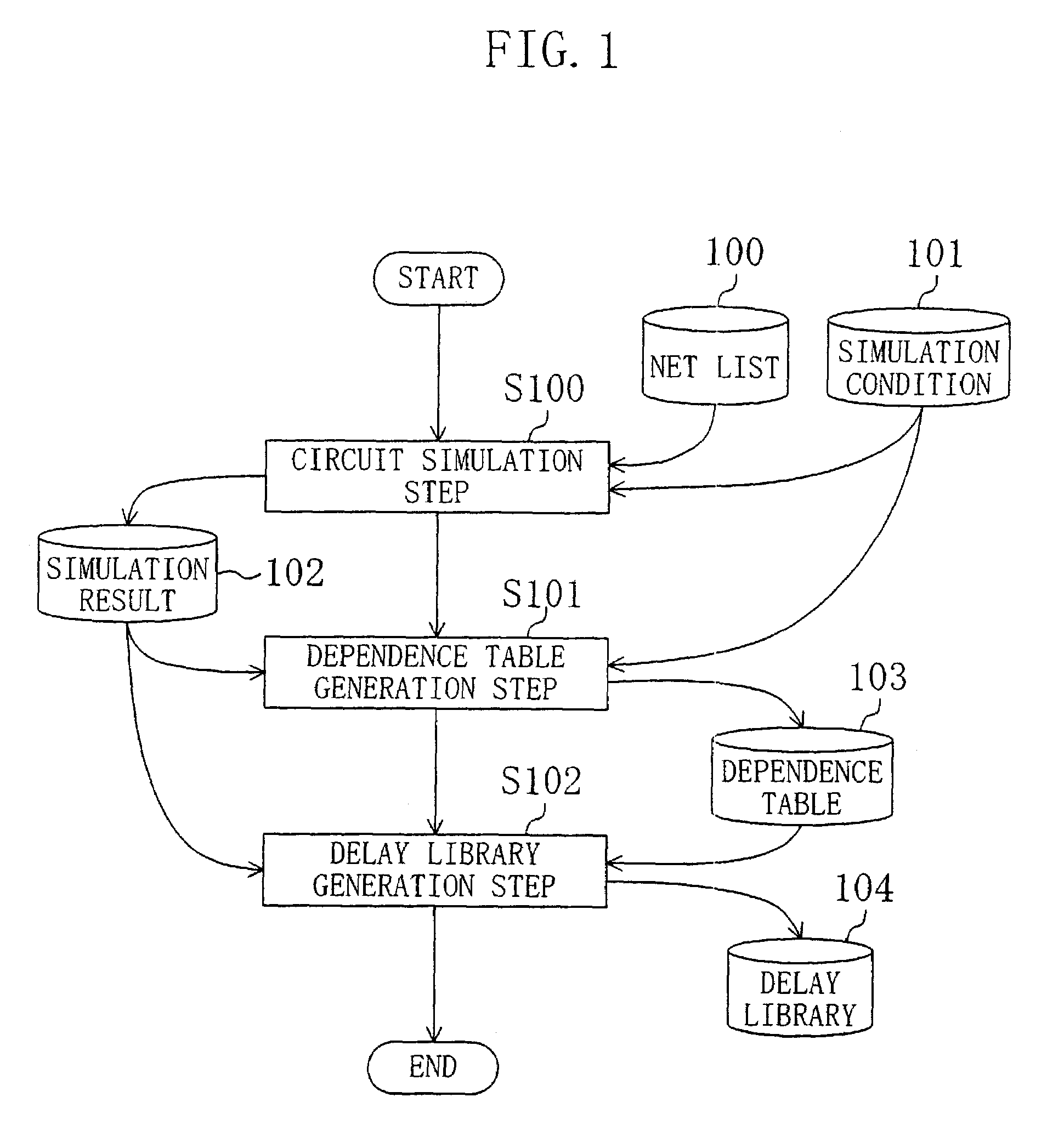
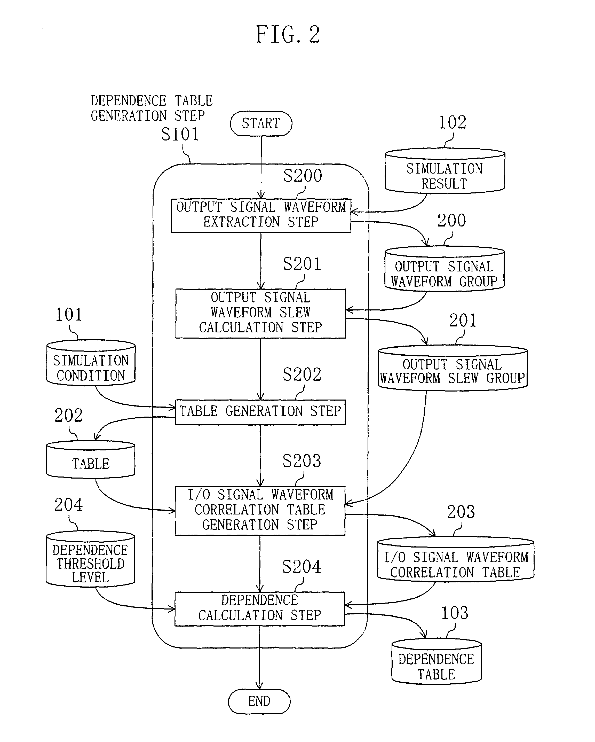
[0073]FIG. 1 shows a procedure of generating a delay library in a cell delay calculation method in accordance with a first embodiment of the present invention. Here, a technique of generating a delay library for a cell exemplarily shown in FIG. 3 will be described concretely. Shown in FIG. 3 are a cell (instance) 300, an input signal waveform group 301 of input signal waveforms that are fed to the instance 300, a load capacitance group 302 of load capacitances that are connected to an output terminal of the instance 300, an output signal waveform 303 which is one of output signal waveforms in an output signal waveform group 200, a voltage level 304 for use in linear approximation, and a linearly-approximated waveform 305 which is a linear approximation of the output signal waveform 303.

[0074]Firstly, in a circuit simulation step S100, a net list 100 at the transistor level and a simulation condition 101 for the cell 300 of FIG. 3 are input to perform a circuit simulation with a circ...

embodiment 2

[0122]A second exemplary embodiment of the present invention will be described below with reference to the drawing figures.

[0123]FIG. 11 shows a semiconductor integrated circuit layout optimization method in accordance with the second embodiment of the present invention. In accordance with the present embodiment, at least one of the input slew rate and the load capacitance of an instance is controlled when performing a timing driven layout, thereby to generate a layout suitable for the delay calculation algorithm of a delay calculation tool that is used at the time of post-layout back annotation.

[0124]In the following description, an example case will explained in which the aforesaid delay calculation algorithm is one that does not deal with the signal waveform propagation between the input and output terminals of an instance.

[0125]Referring to FIG. 11, in a layout step S1100 a net list 1101 and a delay library 1100 are first input for placement / wire routing and thereafter resistanc...


PUM


Abstract

In a circuit simulation step, a cell transistor level net list is input, the slew of an input signal waveform and the magnitude of a load capacitance connected to a cell output terminal are varied for each cell, to perform a circuit simulation of each cell for obtaining an output signal waveform. Next, in a dependence table generation step, the dependence of the output signal waveform slew upon the input slew rate and the load capacitance is calculated for each cell, the dependence thus calculated is compared with a predetermined threshold level, and according to the dependence level, a delay calculation expression with consideration taken to the delay of signal propagation between the cell input and output terminals and another without such consideration are selectively used. Accordingly, the delay times of the cells forming a semiconductor integrated circuit can be calculated at high accuracy and at high processing speed.

Description

[0001]This application is a divisional of application Ser. No. 09 / 714,095, filed Nov. 17, 2000 now U.S. Pat. No. 6,718,529.BACKGROUND OF THE INVENTION[0002]The present invention relates to a delay calculation method and to a layout optimization method for high-accuracy delay time calculation of cells and wires in timing verification during the design of a semiconductor integrated circuit.[0003]Today, because of advances in semiconductor process technology, the size of transistors have been miniaturized and reduced down to less than 0.5 μm (submicron size). Also with respect to rooting of wires, both the wire pitch and the wire width tend toward being shrunk. Therefore, when calculating a length of time taken for a signal to propagate in a large-scale integrated circuit (hereinafter called the “delay time”), it now becomes necessary to pay attention to the influence of the resistance of a wire and the influence of an adjacent wire. These influences have not been taken into much consi...

Claims


Application Information

Patent Timeline
Patent Type & Authority Patents(United States)
IPC IPC(8): G06F17/50G06F9/45G01R31/28H01L21/82H03K19/094H03K19/20
CPCG06F17/5022G06F30/33
Inventor IWANISHI, NOBUFUSA
Owner SOCIONEXT INC
Why Eureka
Try Eureka