Manufacturing method of semiconductor device, semiconductor device, circuit substrate and electronic equipment

a manufacturing method and semiconductor technology, applied in semiconductor/solid-state device testing/measurement, semiconductor devices, semiconductor/solid-state device details, etc., can solve the problems of difficult to form wiring or the like on a polished surface, difficult to mount the electronic parts in the mounting space, and achieve the effect of inexpensive high-performance devices

Active Publication Date: 2006-09-19
SAMSUNG ELECTRONICS CO LTD
View PDF7 Cites 14 Cited by
  • Summary
  • Abstract
  • Description
  • Claims
  • Application Information

AI Technical Summary

Benefits of technology

[0012]In the present method, since the active surface of the substrate finally becomes the mounting surface, by simultaneously forming the coupling terminal or the like and the rearrangement wiring or the like on the active surface side in advance, the step can be simplified as compared to the conventional one (that is, the case in which the chip is three-dimensionally mounted on the active surface side of the substrate and making the back surface side of the substrate the mounting surface). Moreover in the present method, since the rearrangement wiring or the like is formed on the active surface side of the substrate, it becomes easier to form as compared to the conventional case in which the rearrangement wiring or the like is formed on the back surface side (polishing surface) of the substrate.
[0015]In the present method, since the substrate is surely held by the sealing member of a thick film that seals the semiconductor chip, when the tip end portion of the blade penetrates from the substrate to the sealing member side, the space between the two does not oscillate. In the cutting step of the substrate, the supporting member for supporting the substrate may be separately prepared, however, in the present method, since the active surface side of the substrate is protected by the sealing member of the thick film, the substrate can be diced using this sealing member as the supporting member. In this way, the step of attaching the supporting member or the like becomes unnecessary, and the step becomes easier.
[0016]Prior to the cutting of the substrate, it is preferable to provide a step for testing each of the semiconductor devices. In this way, as compared with the case in which the testing step is carried out after the cutting of the substrate (that is, once the substrate has been divided into individual semiconductor devices), the testing becomes easier.
[0017]Prior to mounting of the semiconductor chip, it is preferable that the step of testing each electronic circuit formed on the active surface is provided. In mounting the semiconductor chip, the semiconductor chip is mounted only on the electronic circuit that turns out to be non-defective in the testing of the electronic circuit. By sorting out the non-defective circuits in advance, the mounting of the chips thereafter can be carried out without waste. In mounting the semiconductor chips, it is preferable to mount a dummy chip with respect to the electronic circuit that turns out defective in the testing of the electronic circuit. In this way, the flow of the sealing material becomes uniform, and the air bubble is hardly mixed in the sealing member.
[0019]Moreover, the semiconductor device of the present invention is manufactured by the above described method. Moreover, the circuit substrate or the electronic equipment of the present invention is provided with the above described semiconductor device. Accordingly, it is possible to provide an inexpensive high performance device.

Problems solved by technology

Moreover, these electronic parts are extremely limited in the mounting space.
However, it is technically difficult to form a wiring or the like on a polished surface, or the step becomes complicated by forming a new wiring layer.
However, such a dicing tape is required to be thin, so as a result, the substrate as the adhered sometimes cannot be sufficiently held (that is, oscillation occurs between the adhered and the tape).
When such oscillation occurs during cutting, there is a risk of chipping the substrate (chipping) when the tip end portion of the blade penetrates to the tape side from the substrate.

Method used


Image

  • Manufacturing method of semiconductor device, semiconductor device, circuit substrate and electronic equipment
  • Manufacturing method of semiconductor device, semiconductor device, circuit substrate and electronic equipment
  • Manufacturing method of semiconductor device, semiconductor device, circuit substrate and electronic equipment

Examples


Embodiment Construction

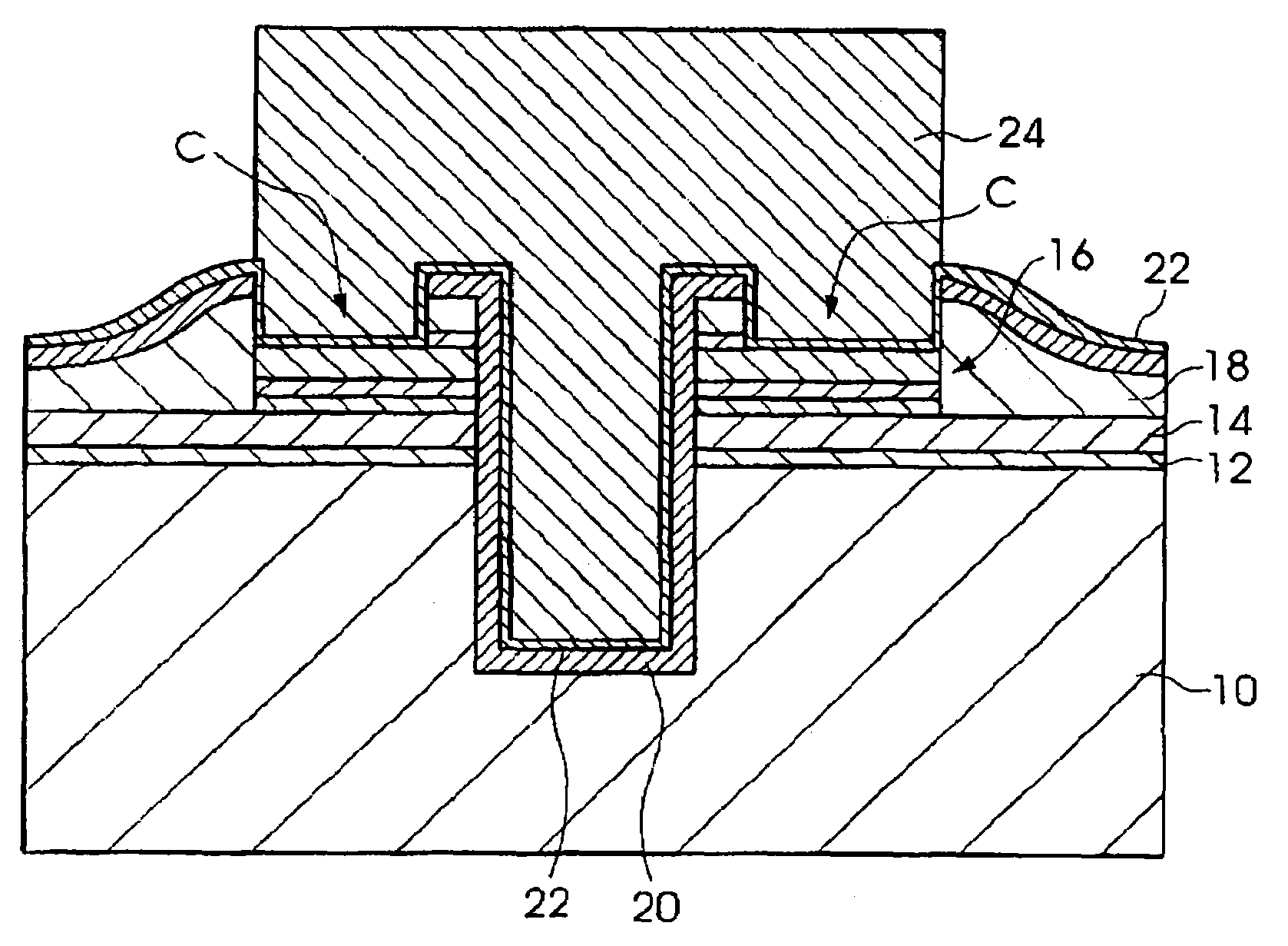
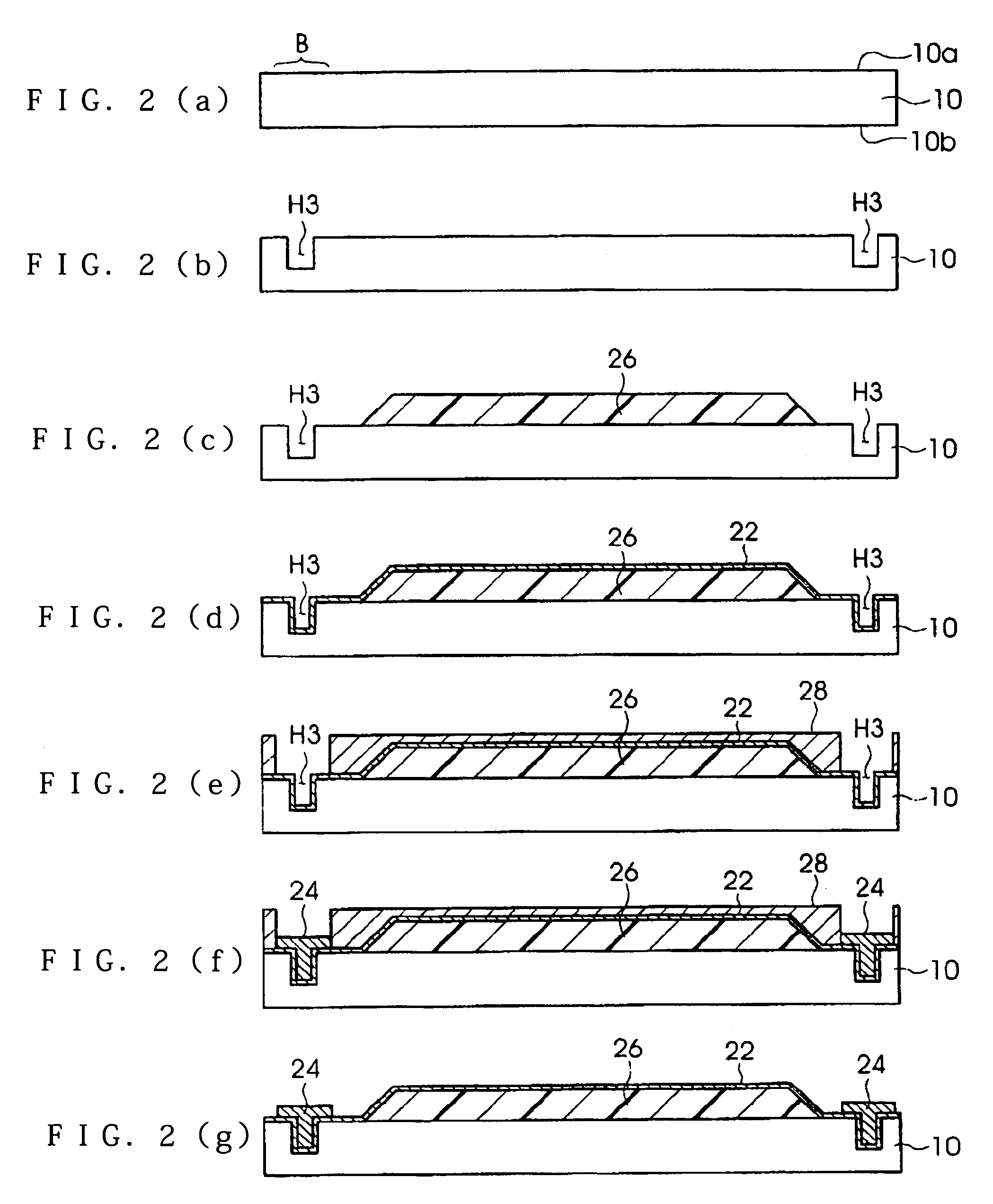
[0036]Hereinafter, referring to the drawing, a manufacturing method of a semiconductor device, a semiconductor device, and electronic equipment will be described in detail according to one embodiment of the present invention. The outline of the manufacturing method of the semiconductor device of the present embodiment has an aspect in the point that an individual semiconductor chip is deposited on a wafer (substrate) that is thinned, and the entire manufacturing step is generally classified into: a first step of processing a substrate on which the semiconductor chip is deposited; a second step of manufacturing the semiconductor chip to be deposited; and a third step of mounting the chip on the substrate. These steps may be carried out sequentially, and the first step and the second step maybe carried out in parallel. In view of the manufacturing efficiency, it is preferable to form the semiconductor chip in the second step in advance, and carry out the third step after the first ste...


PUM


Abstract

A method of manufacturing a semiconductor device is provided. The method includes embedding and forming a coupling terminal as an external electrode of an electronic circuit on an active surface side of a substrate having an active surface formed with a plurality of electronic circuits, exposing a part of the coupling terminal by polishing a back surface side of the substrate, mounting a semiconductor chip on the back surface side of the substrate via the coupling terminal, sealing the semiconductor chip mounted on the substrate by a sealing material, and cutting the substrate for every forming area of each electronic circuit and dividing it into a plurality of semiconductor devices.

Description

RELATED APPLICATIONS[0001]This application claims priority to Japanese Patent Application No. 2003-420807 filed Dec. 18, 2003 which is hereby expressly incorporated by reference herein in its entirety.BACKGROUND[0002]1. Field of the Invention[0003]The present invention relates to a manufacturing method of a semiconductor device, a semiconductor device, a circuit substrate and electronic equipment.[0004]2. Related Art[0005]Currently, since electronic equipment having portability such as a portable phone, a notebook size personal computer, and a PDA (Personal data assistance), and equipment such as a sensor, a micro-machine, and a printer head are small sized and light weight, miniaturization of various electronic parts of a semiconductor chip or the like installed inside have been made. Moreover, these electronic parts are extremely limited in the mounting space.[0006]Therefore, research and development for manufacturing a micro semiconductor chip using a technology called a chip sca...

Claims


Application Information

Patent Timeline
Patent Type & Authority Patents(United States)
IPC IPC(8): H01L21/44H01L21/66H01L21/301H01L21/3205H01L21/768H01L23/12H01L23/48H01L23/52H01L25/00H01L25/065H01L25/07H01L25/18
CPCH01L21/561H01L21/76898H01L23/481H01L25/0657H01L25/50H01L2224/16H01L2225/06513H01L2225/06524H01L2225/06541H01L2225/06582H01L2224/02372H01L2224/05009H01L2224/05548H01L2224/05573H01L2224/05147H01L2224/05647H01L2224/02377H01L2224/05557H01L2224/16146H01L24/81H01L24/16H01L2224/06131H01L24/05H01L2924/00014H01L25/00H01L25/065
Inventor FUKAZAWA, MOTOHIKO
Owner SAMSUNG ELECTRONICS CO LTD
Why Eureka
Try Eureka