Semiconductor device and method of manufacturing the same
Inactive Publication Date: 2006-09-19
FUJITSU SEMICON LTD
View PDF12 Cites 9 Cited by
Summary
Abstract
Description
Claims
Application Information
AI Technical Summary
This helps you quickly interpret patents by identifying the three key elements:
Problems solved by technology
Method used
Benefits of technology
Benefits of technology
[0040]It is an object of the present invention to provide a semiconductor device having a structure, in which the gate electrode employed when the pocket regions connected to the source / drain of the MOS transistor are formed can keep a stable shape, and a method of manufacturing the same.
Problems solved by technology
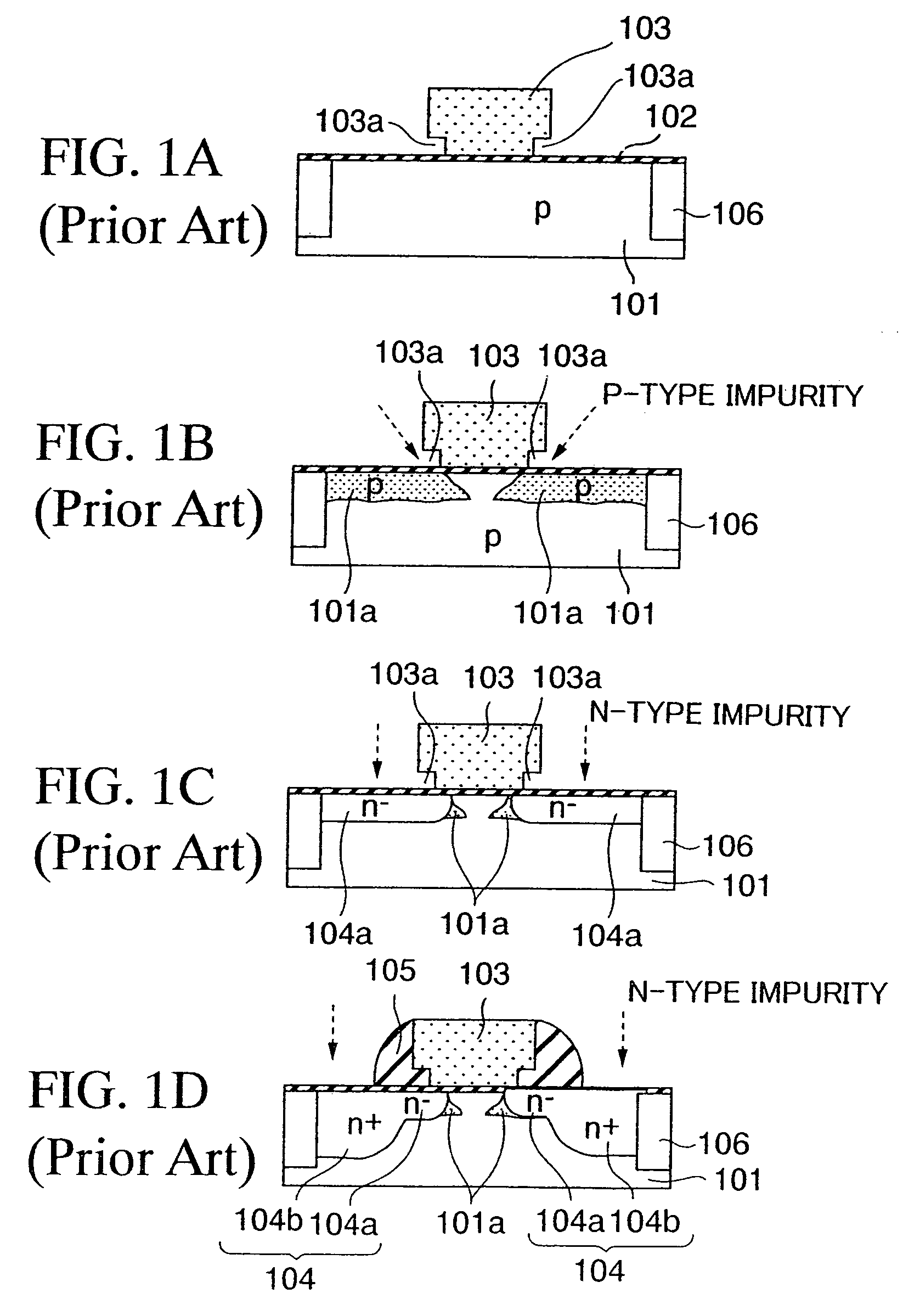
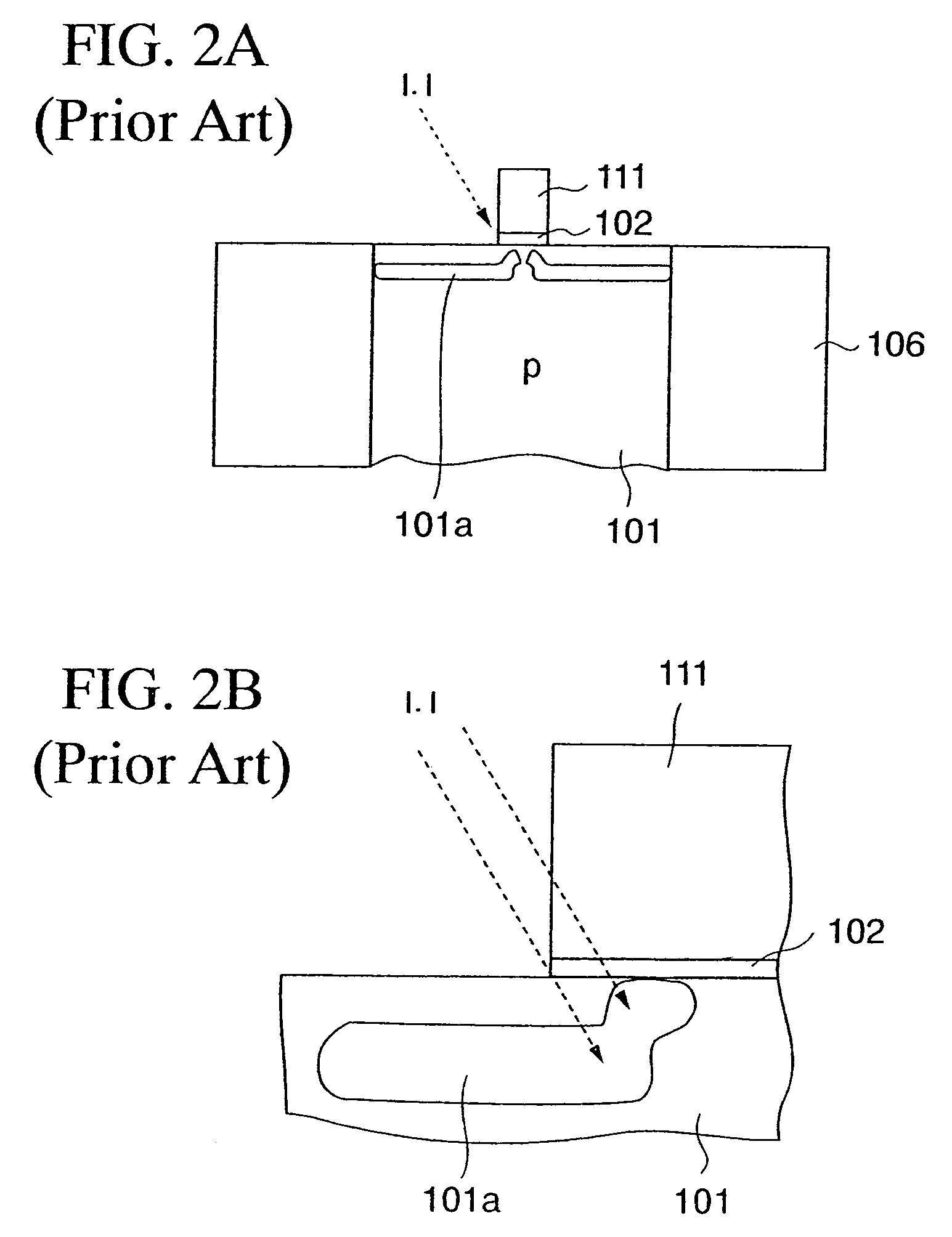
In this manner, if the pocket portions 101a have the concentration distribution close to the channel region under the gate electrode 111, such distribution interferes with the increase of the ON-current and thus the increase in the circuit speed becomes difficult.
In other words, the desired transistor characteristics cannot be obtained by using the normal gate structure having no notch.
Therefore, there is caused the problem that variations in depth and height of the notch portions 103a caused on the substrate surface are increased.
However, if the width of the gate electrode 115g is reduced smaller than 50 nm, for example, it becomes difficult to control the width of the gate electrode 115g by the wet process, so that the variation in the width of plural gate electrodes 115g on the substrate is caused.
Besides, as set forth in Patent Application Publication (KOKAI) Hei 10-294453, it is difficult to form the gate electrodes each having the inverse trapezoid sectional shape in plural in the holes, that are formed in the siliconnitride film to have the inverse trapezoid shape, to have a uniform width.
In addition, since the width of the gate electrode is widened substantially by adding the amorphous silicon film, a distance between the gate electrodes cannot be reduced.
As described above, it turns out that it is difficult to control by the conventional structure the width of gate electrode used as a mask of the ion-implantation at the time of forming a pocket part.
Method used
Image
Click on the blue label to locate the original text in one second.
Reading with bidirectional positioning of images and text.
Examples
first embodiment
[0073](First Embodiment)
[0074]FIGS. 8A to 8C, FIG. 9, FIG. 10, FIG. 11, and FIGS. 12A and 12B are sectional views showing steps of manufacturing a semiconductor device according to a first embodiment of the present invention.
[0075]First, steps required until the structure shown in FIG. 8A is formed will be explained hereunder.
[0076]An STI structure 2 is formed in the device isolation region by forming grooves 1a in the device isolation region, which surrounds an active region A, of a silicon (semiconductor) substrate 1 and then burying an insulating film in the grooves 1a. In this case, in place of the STI structure 2, other device isolation structures such as the device isolation layer formed by the LOCOS method, and others may be employed in the device isolation region.
[0077]Then, a well 3 is formed in the silicon substrate 1 by ion-implanting the impurity into the active region A. The formation of the well 3 is the well-known technology and thus the well 3 can be formed by any of...
second embodiment
[0132](Second Embodiment)
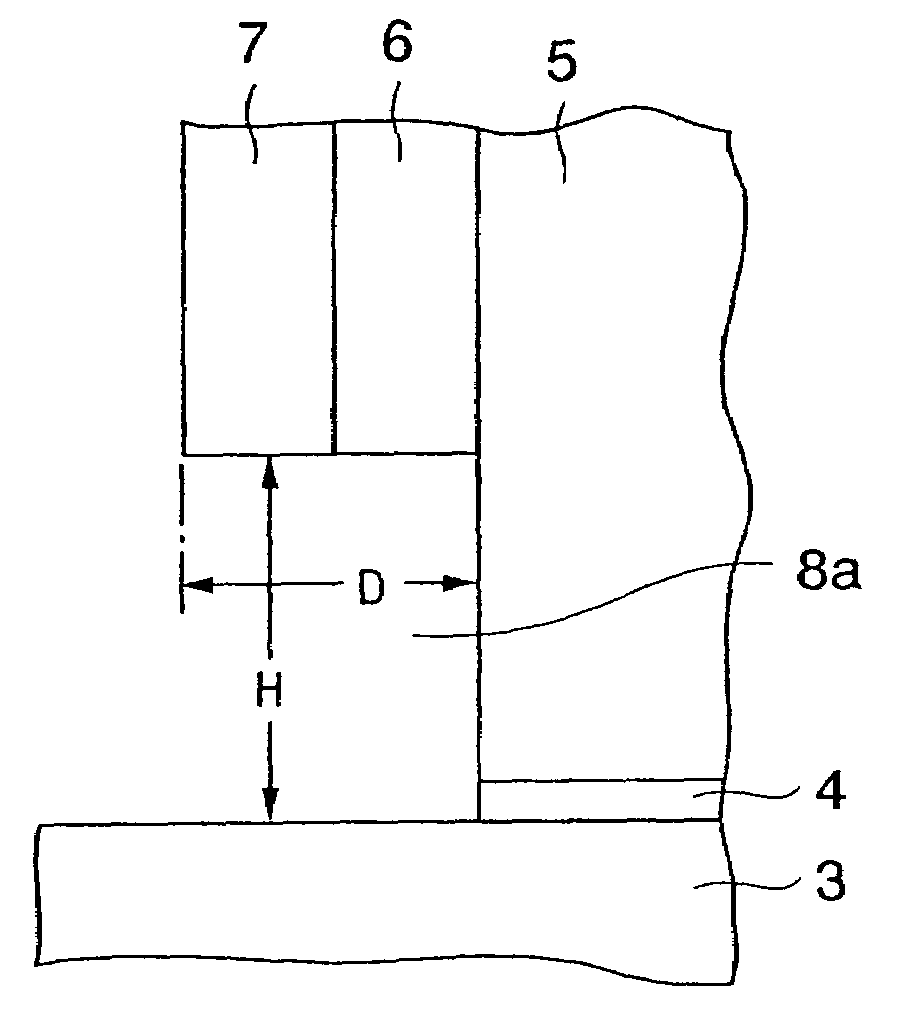
[0133]In the first embodiment, as shown in FIG. 8H, after the notch portion 8a is formed under the ion-implantation controlling film 8 that is formed on the side surfaces of the gate electrode 5, the impurity ion is implanted into the silicon substrate 1 along the oblique direction via the notch portion 8a.
[0134]If the ion-implantation angle to the normal line of the substrate surface is increased, in some cases it is requested that the depth D of the notch portion 8a shown in FIG. 9 should be set larger than the height H.
[0135]The depth D of the notch portion 8a is given by a sum of a thickness of the silicon oxide film 6 and a thickness of the silicon nitride film 7 on the side surface of the gate electrode 5. Also, the height H of the notch portion 8a is given by the thickness of the silicon oxide film 6 on the upper surface of the silicon substrate 1 other than the notch portion 8a.
[0136]Here, if the silicon oxide film 6 is formed thick to increase the...
third embodiment
[0165](Third Embodiment)
[0166]Next, a method of forming another notch portion according to a third embodiment of the present invention will be explained hereunder.
[0167]First, according to the steps described in the first embodiment, the gate electrode 5 is formed on the silicon substrate 1. Then, as shown in FIG. 16A, the silicon oxide film 6 and the silicon nitride film 7 for covering the gate electrode 5 are formed in sequence on the silicon substrate 1. The growth conditions of these films 6, 7 are set identically to those in the first embodiment.
[0168]Then, as shown in FIG. 16B, the silicon oxide film 6 and the silicon nitride film 7 are unisotropically etched in the direction substantially perpendicular to the substrate surface to leave them on the side portions of the gate electrode 5 as the ion-implantation controlling film 8.
[0169]The silicon oxide film 6 is exposed from the lower end of the ion-implantation controlling film 8. Therefore, the silicon oxide film 6 is wet-etc...
PUM
Abstract
There are provided a gate electrode formed on a semiconductor substrate of one conductivity type via a gate insulating film, ion-implantation controlling films formed on both side surfaces of the gate electrode and having a space between the gate electrode and an upper surface of the semiconductor substrate, first and second impuritydiffusion regions of opposite conductivity type formed in the semiconductor substrate on both sides of the gate electrode and serving as source / drain, a channel region of one conductivity type formed below the gate electrode between the first and second impuritydiffusion regions of opposite conductivity type, and pocket regions of one conductivity type connected to end portions of the impuritydiffusion regions of opposite conductivity type in the semiconductor substrate below the gate electrode and having an impurity concentration of one conductivity type higher than the channel region.
Description
CROSS-REFERENCE TO RELATED APPLICATIONS[0001]This application is a DIV of Ser. No. 10 / 261,695 Oct. 2, 2002 now U.S. Pat. No. 6,800,909[0002]This application is based upon and claims priority of Japanese Patent Applications No. 2001-308429 filed in Oct. 4, 2001, and No. 2002-256229, filed in Aug. 30, 2002, the contents being incorporated herein by reference.BACKGROUND OF THE INVENTION[0003]1. Field of the Invention[0004]The present invention relates to a semiconductor device and a method of manufacturing the same and, more particularly, a semiconductor device having one conductivity type impurity regions, that are formed in vicinity of two opposite conductivity type impurity diffusion regions constituting the source / drain in one conductivity type substrate respectively by the pocket injection technology, and a method of manufacturing the same.[0005]2. Description of the Prior Art[0006]The MOS transistor is designed based on the scaling theory. If the MOS transistor whose gate length ...
Claims
Application Information
Patent Timeline
Application Date:The date an application was filed.
Publication Date:The date a patent or application was officially published.
First Publication Date:The earliest publication date of a patent with the same application number.
Issue Date:Publication date of the patent grant document.
PCT Entry Date:The Entry date of PCT National Phase.
Estimated Expiry Date:The statutory expiry date of a patent right according to the Patent Law, and it is the longest term of protection that the patent right can achieve without the termination of the patent right due to other reasons(Term extension factor has been taken into account ).
Invalid Date:Actual expiry date is based on effective date or publication date of legal transaction data of invalid patent.

