Light emitting device and method for manufacturing the same

a technology of light-emitting devices and manufacturing methods, which is applied in the direction of discharge tubes/lamp details, organic semiconductor devices, discharge tubes/lamp details, etc., can solve the problems of reducing the lifetime of light-emitting elements, and reducing the light-emitting efficiency of light-emitting elements

Active Publication Date: 2006-09-19
SEMICON ENERGY LAB CO LTD
View PDF18 Cites 52 Cited by
  • Summary
  • Abstract
  • Description
  • Claims
  • Application Information

AI Technical Summary

Benefits of technology

[0019]Since the height of the second sealing agent immediately after application is larger than that of the first sealing agent, when the two pieces of substrates are adhered to each other, the second sealing agent is pressed and spread so as to cover the pixel portion prior to the first sealing agent. At this moment, the pixel portion can be surely covered with the second sealing agent due to the arrangement of the pair of first patterns. Further, after the second sealing agent is spread on the entire surface of the pixel portion, the first sealing agent is subsequently spread. At this moment, gaps in the vicinity of each midpoint of the two sides for the second pattern formed along the pair of first patterns are filled, respectively. The second sealing agent is completely shielded from the outside air by the first sealing agent. Therefore, it is possible to prevent moisture and oxygen from reaching into the EL element by both of the first sealing agent and the second sealing agent.
[0024]In the case of sealing an EL element for the top emission structure or the dual emission structure, the second sealing agent is cured by heating rather than by UV irradiation. Accordingly, the pixel portion is not damaged by the UV irradiation, and hence, the problems of decreasing luminance of the EL element and shortening lifetime thereof can be solved.
[0025]According to the invention as disclosed in the specification, in the sealing step of the top emission structure and the dual emission structure, the sealing agent covering the pixel portion can be cured without damaging the EL element due to UV irradiation even in the case of using a sealing device that only has a function of UV irradiation. As a result, a light emitting device with high reliability can be obtained.
[0026]Since the first sealing agent in the periphery of the pixel portion is cured at short times by being irradiated with UV light prior to the second sealing agent, after curing the first sealing agent, the first sealing agent and the second sealing agent are not mixed with each other even if they are in contact with each other for a long time. Therefore, the sealing materials are not deformed and the adhesive strength thereof is not degraded, thereby providing a light emitting device with higher reliability.
[0027]Furthermore, since the second pattern of the first sealing agent is continuously formed, the second pattern of the first sealing agent allows the second sealing agent to be shielded from the outside air completely. Consequently, it is possible to prevent moisture or oxygen from reaching into the EL element by both the first sealing agents and second sealing agent. As a result, a light emitting device with higher reliability can be obtained.

Problems solved by technology

Since the EL element is extremely and easily deteriorated by being oxidized or absorbing moisture due to existence of oxygen or moisture, there has been a problem that the light-emitting efficiency of the EL element is decreased or the lifetime thereof is shortened.
Further, since an EL material is damaged by UV irradiation, there has been a problem in which the light-emitting efficiency of a light emitting element is reduced and lifetime thereof is shortened.
However, in the case of a structure in which an electrode is formed as an anode over a substrate, a layer containing an organic compound is formed on the anode, and a cathode that is a transparent electrode is formed on the layer containing the organic compound (hereinafter, the structure is referred to as a top emission structure), an opposing substrate made from a light shielding material cannot be used.
Further, in the case of the top emission structure and the dual emission structure, when the drying agent is arranged on a pixel portion, the drying agent hinders display.
When oxygen and moisture exist therein, a problem in which the EL element is deteriorated has been caused.
In the case of using such sealing devices, however, the heat-curable sealing agent cannot be used therein.
Further, since the EL element is damaged by UV irradiation and thermal shock, there has been a problem of decreasing the luminance for the EL element and a problem of shortening its lifetime.
When sealing materials before being cured are in contact with each other for a long time, the sealing materials are likely to be mixed with each other, which result in deformation.
Further, since a mixed portion of the mixed sealing materials is not cured uniformly, the adhesive strength is likely to be reduced.

Method used


Image

  • Light emitting device and method for manufacturing the same
  • Light emitting device and method for manufacturing the same
  • Light emitting device and method for manufacturing the same

Examples


embodiment mode 1

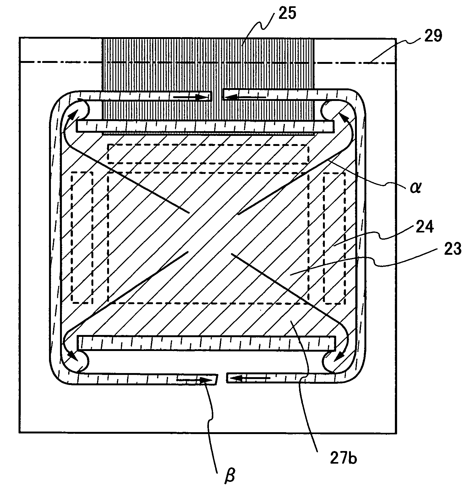
[0038]FIG. 1 is a top view of an active matrix light emitting device according to the present invention as disclosed in the specification.

[0039]In FIG. 1A, reference numeral 11 denotes a first substrate; 12, a second substrate; 13, a pixel portion; 14, a driver circuit portion; 15, a terminal portion; each of 16a and 16b; a first sealing agent; and 17a, a second sealing agent.

[0040]Though the material for the first substrate 11 is not particularly limited, the first substrate is preferably formed of a material having a same thermal expansion coefficient as that of the second substrate 12 from the viewpoint of attaching to the second substrate 12. In the case of the bottom emission structure, the first substrate 11 is formed of a substrate having a light transmitting property such as a glass substrate, a quartz substrate, and a plastic substrate. In the case of the top emission structure, a semiconductor substrate, a metal substrate, and the like can be used, too. Further, in the cas...

embodiment mode 2

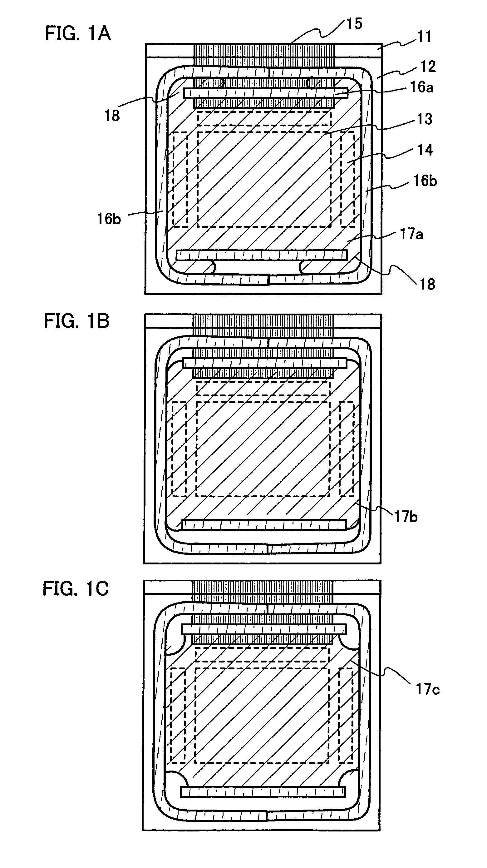
[0053]A part of the cross sectional structure of a pixel portion according to the present invention as disclosed in the specification will hereinafter be described with reference to FIG. 3A.

[0054]In FIG. 3A, reference numeral 300 denotes a first substrate; each of 301a and 301b, an insulating layer; 302, a TFT; 308, a first electrode; 309, an insulator; 310, an EL layer; 311, a second electrode; 312, a transparent protective layer; 313, a second sealing agent; and 314, a second substrate.

[0055]The TFT (a p-channel TFT) 302 formed over the first substrate 300 is an element for controlling the electric current flowing through the EL layer 310 that emits light. Reference numeral 304 denotes a drain region (or a source region). Reference numeral 306 denotes a drain electrode (or a source electrode) for connecting the first electrode and the drain region (or the source region). Further, a wiring 307 such as a power supply line and a source wiring is formed simultaneously with the drain e...

embodiment mode 3

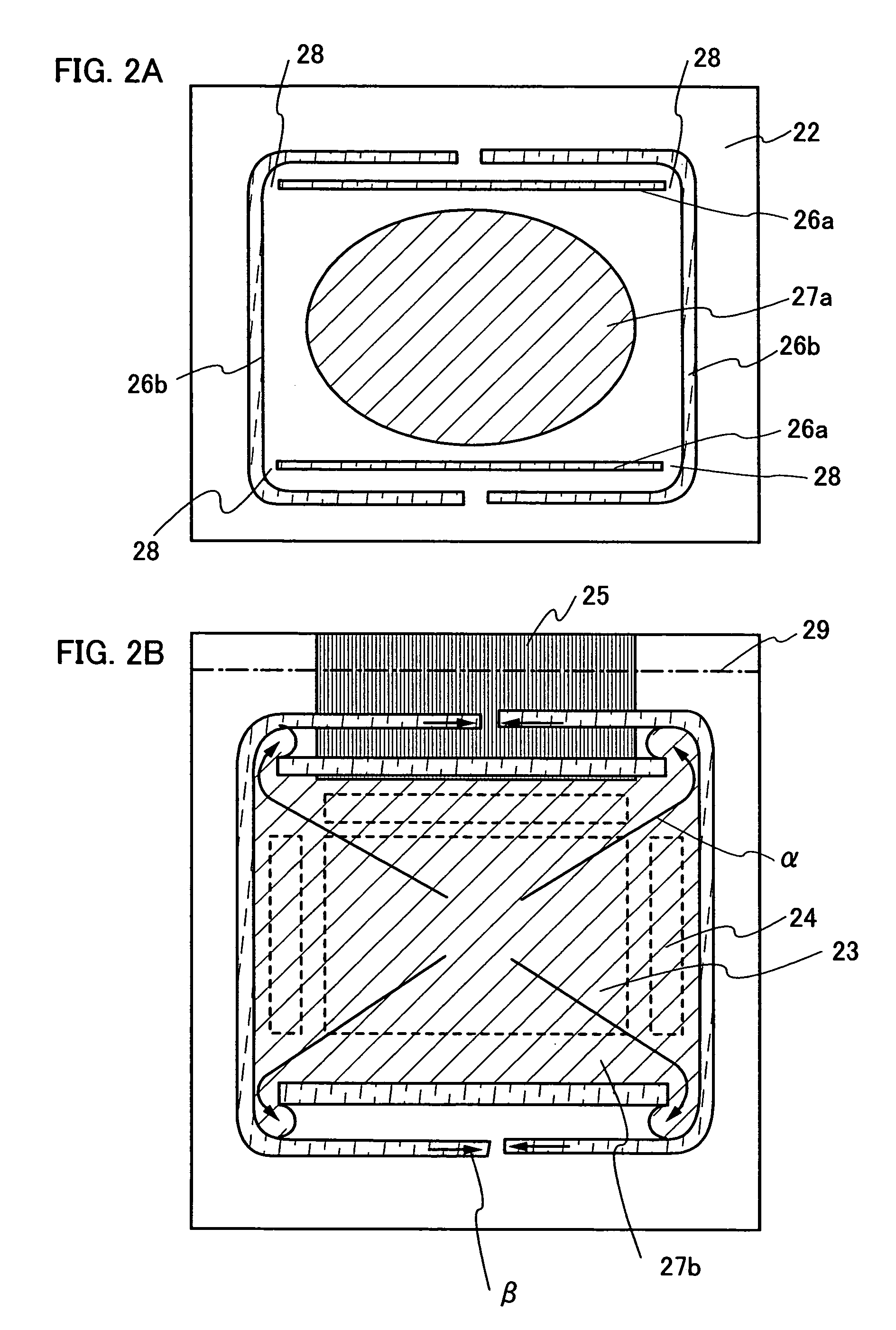
[0072]FIG. 4 shows a case of forming a plurality of pixel portions on one substrate, that is, an example of multiple patterns. An example of forming four panels on one substrate is shown here.

[0073]As illustrated in FIG. 4A, a first sealing agent having first patterns 32a and second patterns 32b is formed in predetermined positions over a second substrate 31 under an inert gas atmosphere by using a dispenser apparatus. As for the first translucent sealing agent 32a and 32b, a material including filler (6 μm to 24 μm in diameter) with the viscosity of 370 Pa·s is used. Since the first sealing agent 32a and 32b are simple sealing patterns, they can also be formed by the printing technique.

[0074]As depicted in FIG. 4B, a second sealing agent 33, which will have a light transmitting property after being cured, is dropped into each region surrounded by the first patterns 32a and second patterns 32b of the first sealing agent (note that, openings are formed between the edges of the first ...


PUM


Abstract

When attaching a substrate with an EL element formed thereon and a transparent sealing substrate, the periphery of a pixel portion is surrounded with a first sealing agent that maintains a gap between the two pieces of substrates, an entire surface of the pixel portion is covered with a second transparent sealing agent so that the two pieces of substrate is fixed with the first sealing agent and the second sealing agent. Consequently, the EL element can be encapsulated by curing the first sealing agent and the second sealing agent without enclosing a drying agent and doing damage to the EL element due to UV irradiation even when a sealing device only having a function of UV irradiation is used.

Description

TECHNICAL FIELD[0001]The present invention relates to a light emitting device having a light emitting layer which includes an organic compound, and a method for manufacturing the same. The present invention further relates to an electronic appliance mounted with the light emitting device as a component. The light emitting device described in the present specification indicates, for example, an EL display device.BACKGROUND OF THE INVENTION[0002]In recent years, research related to a light emitting device having an EL element as a self-luminous element has been actively carried out. Particularly, a light emitting device using an organic material as an EL material has been attracting attention. The light emitting device is also referred to as an EL display device. The EL element includes a layer containing an organic compound, which generates luminescence (electroluminescence) by being applied with an electric field (hereinafter, referred to as an EL layer); an anode; and a cathode. Th...

Claims


Application Information

Patent Timeline
Patent Type & Authority Patents(United States)
IPC IPC(8): H05B33/04H01L27/32H01L51/52
CPCH01L51/5237H01L51/5256H05B33/04H01L27/322H01L27/3244H01L2251/5315H01L2251/5323H01L51/5271H10K59/38H10K59/12H10K50/856H10K50/8426H10K2102/3026H10K2102/3031H10K50/846H10K50/8445H10K59/1213H10K71/00
Inventor KURIHARA, TOMOYUKI
Owner SEMICON ENERGY LAB CO LTD
Why Eureka
Try Eureka