

Method of producing a high resistivity SIMOX silicon substrate
a technology of simox silicon and high resistivity, which is applied in the direction of electrical apparatus, semiconductor devices, semiconductor/solid-state device details, etc., can solve the problems of reducing the electrical resistivity of the wafer, adversely affecting the electrical isolation of different devices formed on the wafer, and affecting the stability of electrical resistivity, etc., to achieve the effect of improving the stability of the resistivity of the simox wafer and high electrical resistivity
- Summary
- Abstract
- Description
- Claims
- Application Information
AI Technical Summary
Benefits of technology
Problems solved by technology
Method used
Image

Examples
example 1
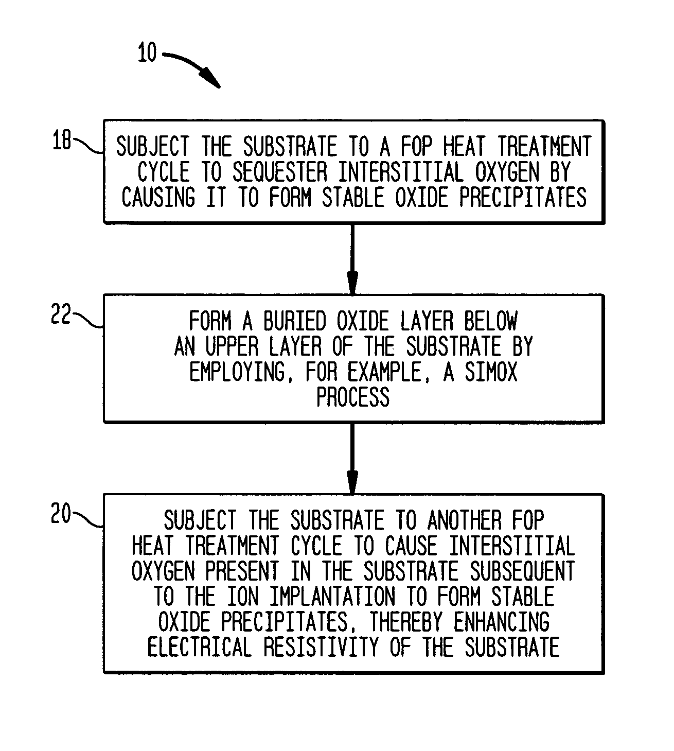
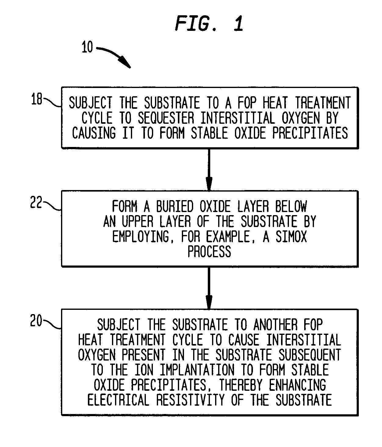
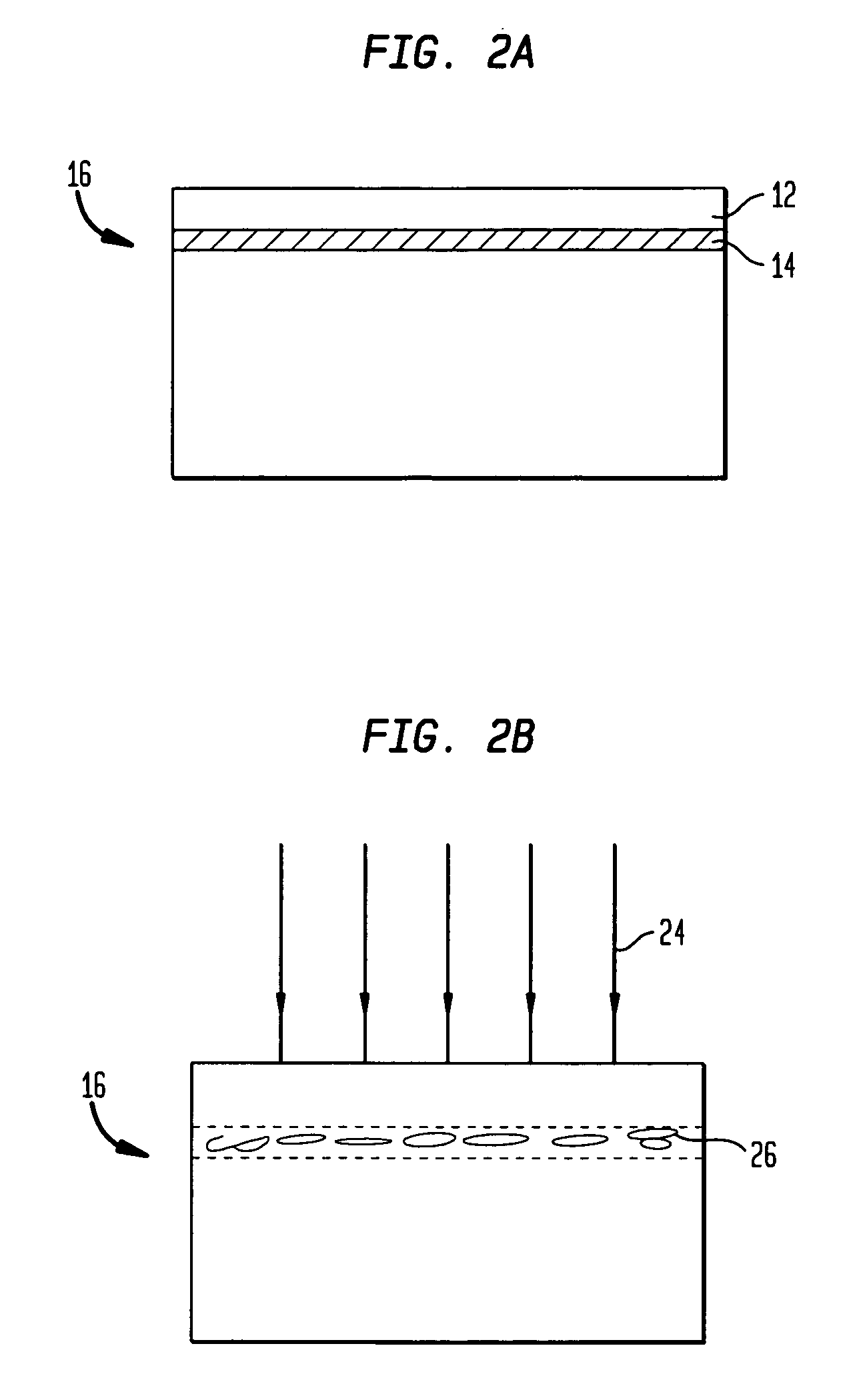
[0047]A silicon wafer cut from a single silicon crystal formed by CZ method was subjected to a ‘denuding’ process by being maintained at a temperature of about 1000 C for approximately 3 hours. The ‘denuding’ process diminishes interstitial oxygen concentration in a substrate layer proximate to the substrate surface. It should be understood that the methods of the invention can be practiced on a silicon substrate without subjecting the substrate to a denuding step.
[0048]Subsequently, the substrate was subjected to a FOP heat treatment protocol by being maintained at an initial elevated temperature of approximately 650 C for about 6 hours. The substrate was then subjected to a temperature of about 800 C for approximately 6 hours, followed by a temperature of about 1000 C for approximately 16 hours. The FOP heat treatment, as discussed above, causes the interstitial oxygen atoms / ions to form stable oxide precipitates, thereby lowering the interstitial oxygen concentration in the subst...
example 2
[0052]A silicon wafer can be subjected to an FOP heat treatment protocol by being maintained at an initial elevated temperature of approximately 650 C for about 6 hours. The substrate can then be subjected to a temperature of about 800 C for approximately 6 hours, followed by a temperature of about 1000 C for approximately 16 hours.
[0053]Subsequently, a selected dose of oxygen ions, for example, a dose of about 3×1017 cm−2 can be implanted in the wafer by exposing the wafer to a beam of oxygen ions having an energy of approximately 200 keV to form a buried oxygen rich damaged layer in the substrate.
[0054]The substrate can then be annealed at a temperature of 1300 C for about 10 hours to generate a continuous buried oxide layer in the oxygen rich damaged layer.
[0055]With reference to FIG. 7, a second FOP heat treatment protocol can be integrated in a ramp down of the substrate temperature after the completion of the annealing step at 1300 C. In particular, subsequent to the completio...
PUM
| Property | Measurement | Unit |
|---|---|---|
| energy | aaaaa | aaaaa |
| temperature | aaaaa | aaaaa |
| temperature | aaaaa | aaaaa |
Abstract
Description
Claims
Application Information