Method of manufacturing liquid crystal display

a technology of liquid crystal display and liquid crystal display, which is applied in the direction of electrical equipment, semiconductor devices, instruments, etc., to achieve the effects of enhancing the brightness of images displayed on the screen, enhancing the aperture ratio, and increasing the light transmittance of liquid crystal display

Active Publication Date: 2006-09-26
HANNSTAR DISPLAY CORPORATION
View PDF4 Cites 27 Cited by
  • Summary
  • Abstract
  • Description
  • Claims
  • Application Information

AI Technical Summary

Benefits of technology

[0013]An objective of the present invention is to provide a method of manufacturing a liquid crystal display with a high aperture ratio. Because the aperture areas are not covered with any gate insulating layer or any inorganic passivation layer, the light transmittance of the liquid crystal display increases so as to enhance the brightness of the images displayed on the screens.

Problems solved by technology

However, as regards the layers deposited on the gate pads and the gate electrodes, etching only takes place in the layers above the semiconductor layer.

Method used


Image

  • Method of manufacturing liquid crystal display
  • Method of manufacturing liquid crystal display
  • Method of manufacturing liquid crystal display

Examples


Embodiment Construction

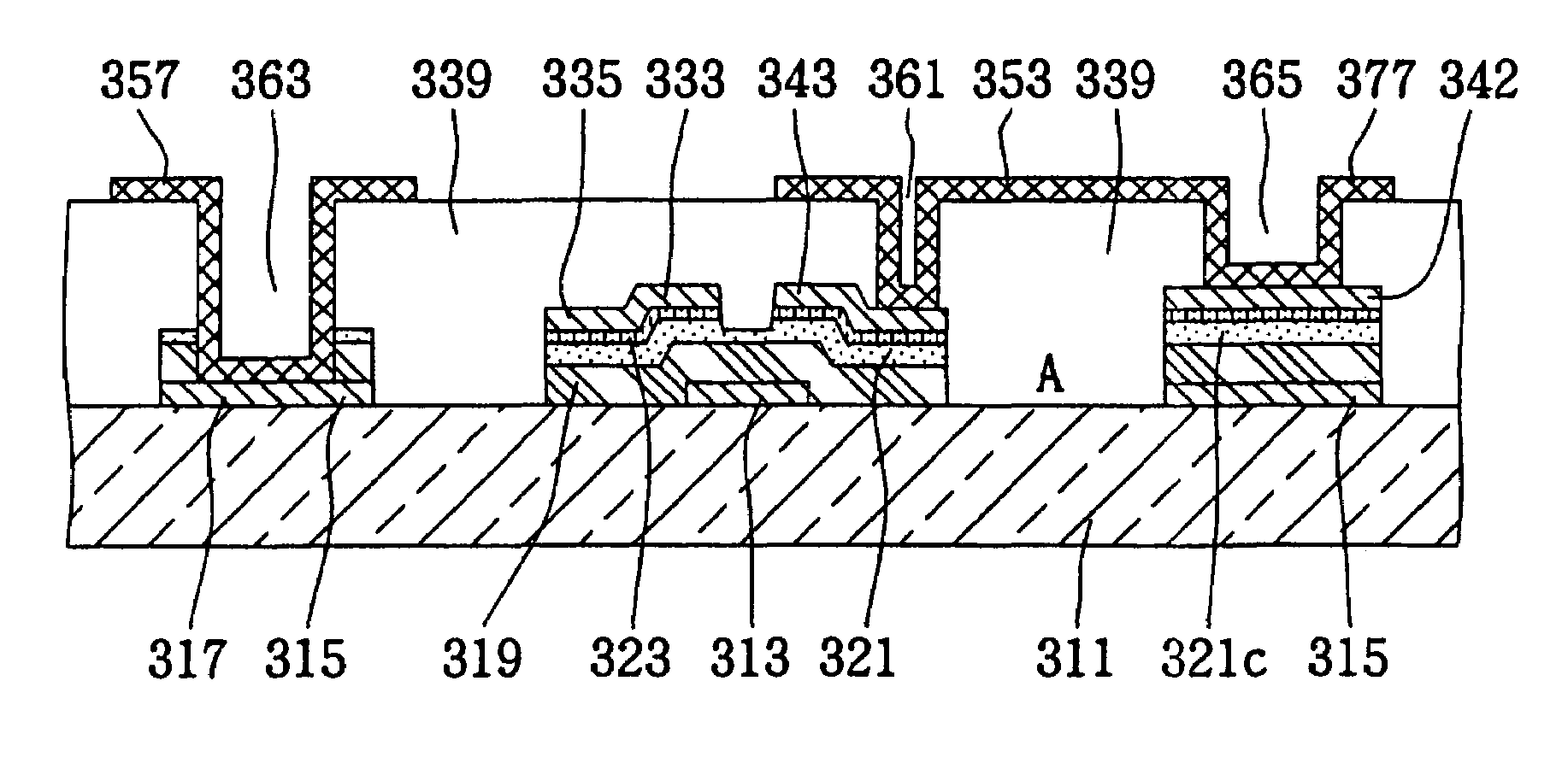
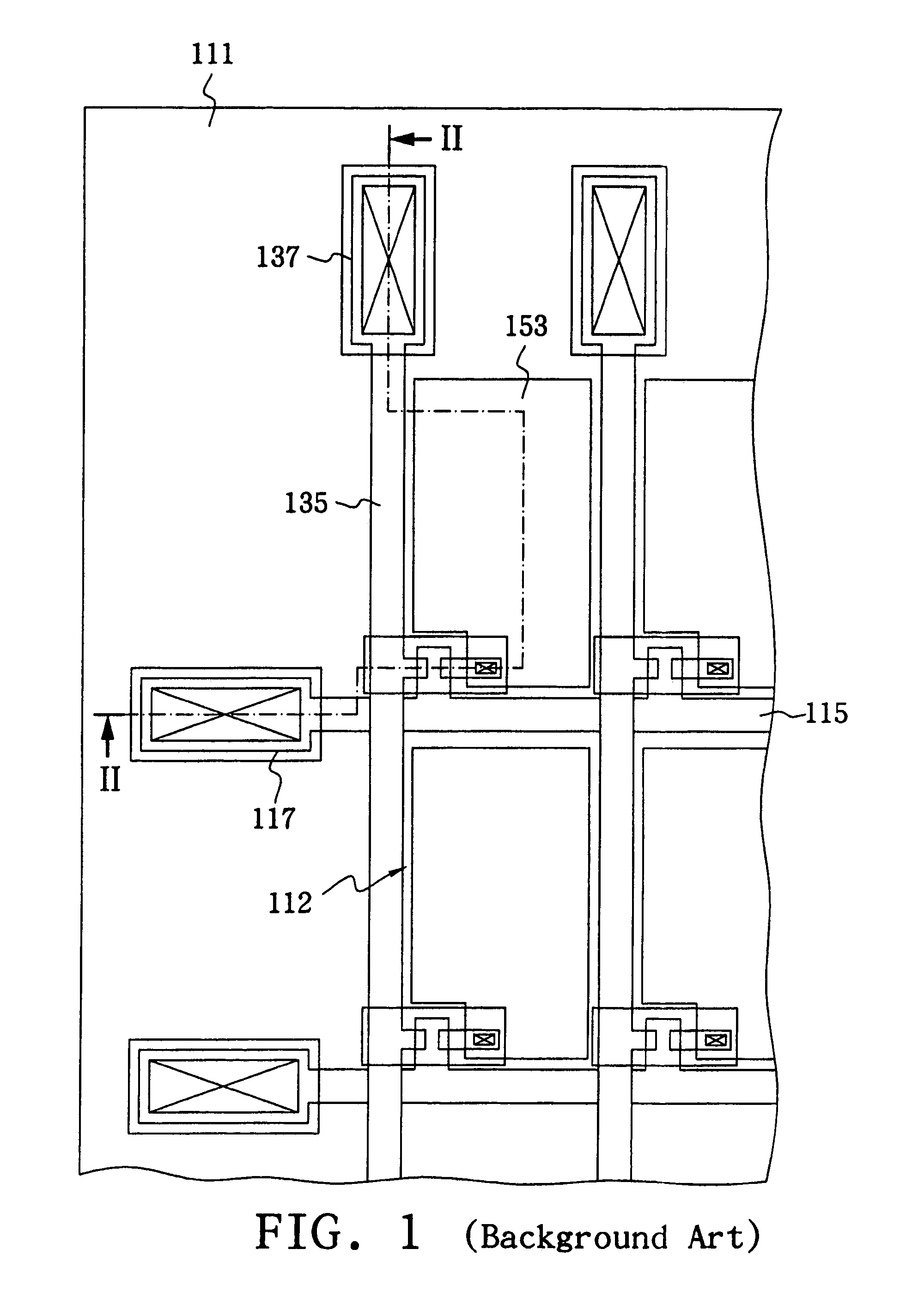
[0026]FIG. 3 is a schematic diagram of the partial circuit of an active substrate in accordance with the present invention. On a substrate 311 are a plurality of pixels 312 disposed at the intersections of the scanning lines 315 and the data lines 335. A gate pad 317 and a data pad 337 are formed at one end of each scanning line 315 and each data line 335 respectively. Various driving devices are connected to the gate pads 317 and the data pads 337. Inside each pixel 312 is a thin film transistor 314 which controls. Signal voltages of the data lines 335 may be written into the pixel electrodes 353 through the scanning lines 315. To prevent the voltages written into the pixel electrodes 353 from attenuating excessively with time, a storage capacitor 316 is formed either between a scanning line 315 and a pixel electrode 353 or between a scanning line 315 and a common electrode.

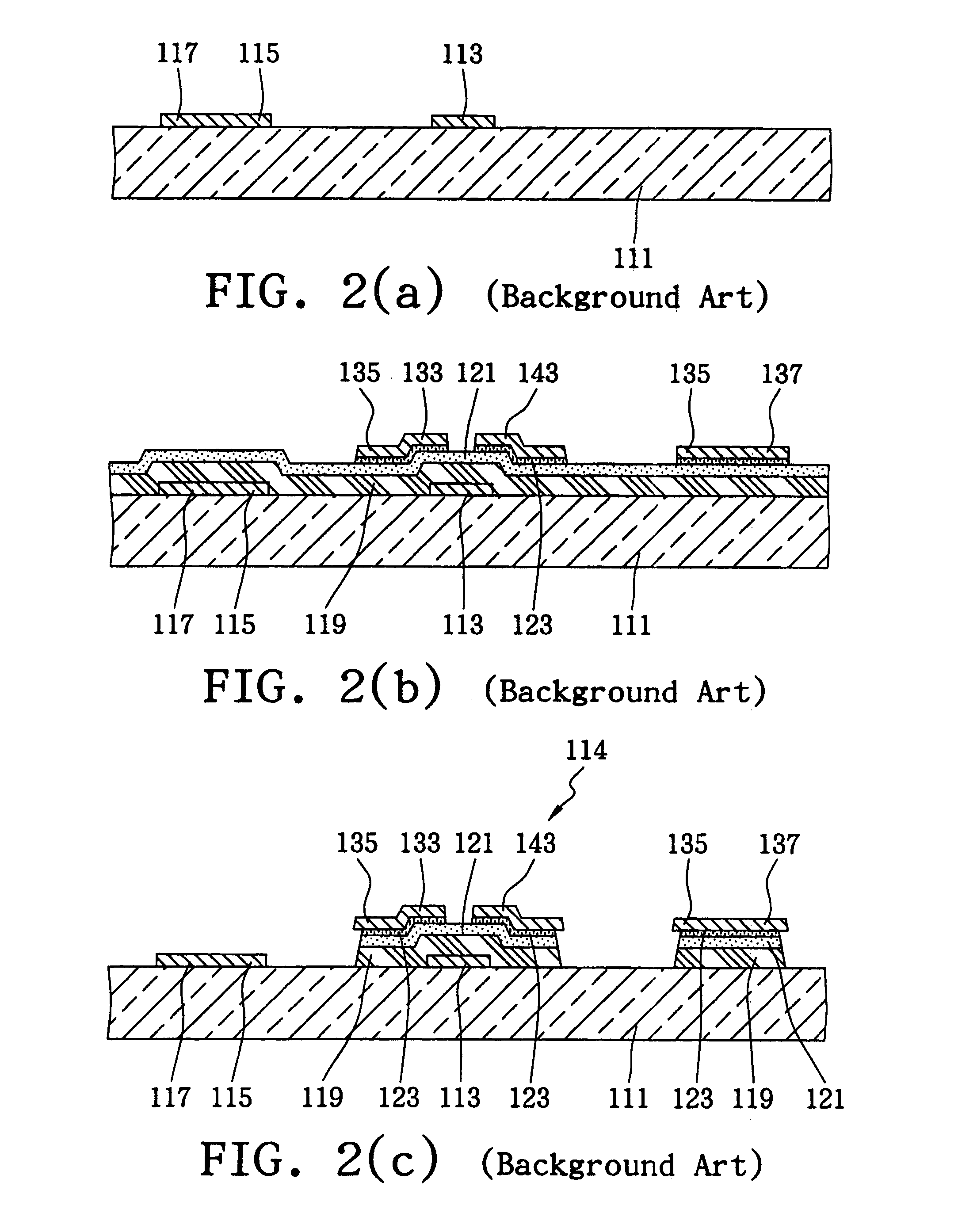
[0027]FIGS. 4(a)–4(e) are cross-sectional diagrams taken along the line III—III, regarding the steps of the m...


PUM

PropertyMeasurementUnit
conductiveaaaaaaaaaa
thicknessesaaaaaaaaaa
thicknessaaaaaaaaaa

Abstract

On a substrate, the pattern of the first conductive layer is defined, that is, a gate line combination including gate pads, scanning lines and gate electrodes. A gate insulating layer, a semiconductor layer, a doped semiconductor layer and a second conductive layer are deposited on the substrate and the above-mentioned gate line combination in sequence. A photoresist layer is overlaid on the second conductive layer. The photoresist layer within the aperture areas is fully exposed. Using a half-tone mask or a slit pattern to make parts of the photoresist layer lying on the gate pads and the gate electrodes are not exposed to its full depth. As a result, the photoresist pattern formed varies in thickness. After being processed with drying etching and wet etching for several times, all the layers previously deposited within the aperture areas can be totally etched and removed. However, as regards the layers deposited on the gate pads and the gate electrodes, etching only takes place in those layers above the semiconductor layer. Then, an organic protection layer is laid on the substrate and the above-mentioned structure, and the holes, which are to function as the passageways for the transparent conductive layer to contact the metallic layer, are defined on the organic protection layer. Then, the gate pads are exposed out of holes above them, using dry etching again. Lastly, the pattern of the transparent conductive layer is defined on the organic protection layer and in the plurality of holes.

Description

BACKGROUND OF THE INVENTION[0001]1. Field of the Invention[0002]The present invention relates to a method of manufacturing liquid crystal displays, and more particularly, to a method for the planarization manufacturing of a high-transmittance liquid crystal display.[0003]2. Description of the Related Art[0004]There is an ever-increasing luminance requirement for products related to a liquid crystal display (LCD) available on the market, such as a desktop LCD, a notebook LCD, and an LCD TV. In order to meet the high-luminance requirement, LCD panel manufacturers envision an increase in the aperture ratio of LCD panels and the light transmittance of aperture areas in the hope of increasing the overall transmittance rate of LCD panels, but they are reluctant to pursue the goal at the expense of power consumption.[0005]As regards the manufacturing processes and patents intended for high aperture ratios as put forth by TFT-LCD manufacturers in Japan and South Korea, they essentially invo...

Claims


Application Information

Patent Timeline
Patent Type & Authority Patents(United States)
IPC IPC(8): H01L21/76H01L21/00G02F1/1362G02F1/1368H01L21/77H01L21/84
CPCG02F1/13458G02F1/136227H01L27/1214G02F1/1368G02F2001/136236H01L27/1288G02F1/136236
Inventor LAN, CHIH-CHIEHHUNG, HUNG-YI
Owner HANNSTAR DISPLAY CORPORATION
Why Eureka
Try Eureka