Field emission source with plural emitters in an opening

a field emission source and plural emitter technology, applied in the field of field emission electron sources, can solve the problems of inability to apply voltage sufficient to extract electrodes, inability to obtain large current, and reduced layer, etc., to achieve high mass productivity, reduce cost, and increase current density

Inactive Publication Date: 2006-09-26
NAT INST OF ADVANCED IND SCI & TECH +1
View PDF12 Cites 5 Cited by
  • Summary
  • Abstract
  • Description
  • Claims
  • Application Information

AI Technical Summary

Benefits of technology

[0031]It is an object of the present invention to provide a field emission electron source capable of achieving a large current density at low cost with high mass productivity.

Problems solved by technology

However, since the resistant voltage of the insulating layer is reduced, a voltage sufficient to extract electrodes cannot be applied.
As a result, large current cannot be obtained.
On the other hand, in the fourth conventional example mentioned above, since a general semiconductor manufacturing line does not have an anodic oxidation step, this step is required to be added, thus increasing the cost.
Furthermore, when the anodic oxidation step is actually added, many problems about mass production, for example, controllability of the anodic oxidation step and uniformity of the surface of the porous silicon layer, etc., have to be clarified.

Method used


Image

  • Field emission source with plural emitters in an opening
  • Field emission source with plural emitters in an opening
  • Field emission source with plural emitters in an opening

Examples


embodiment 1

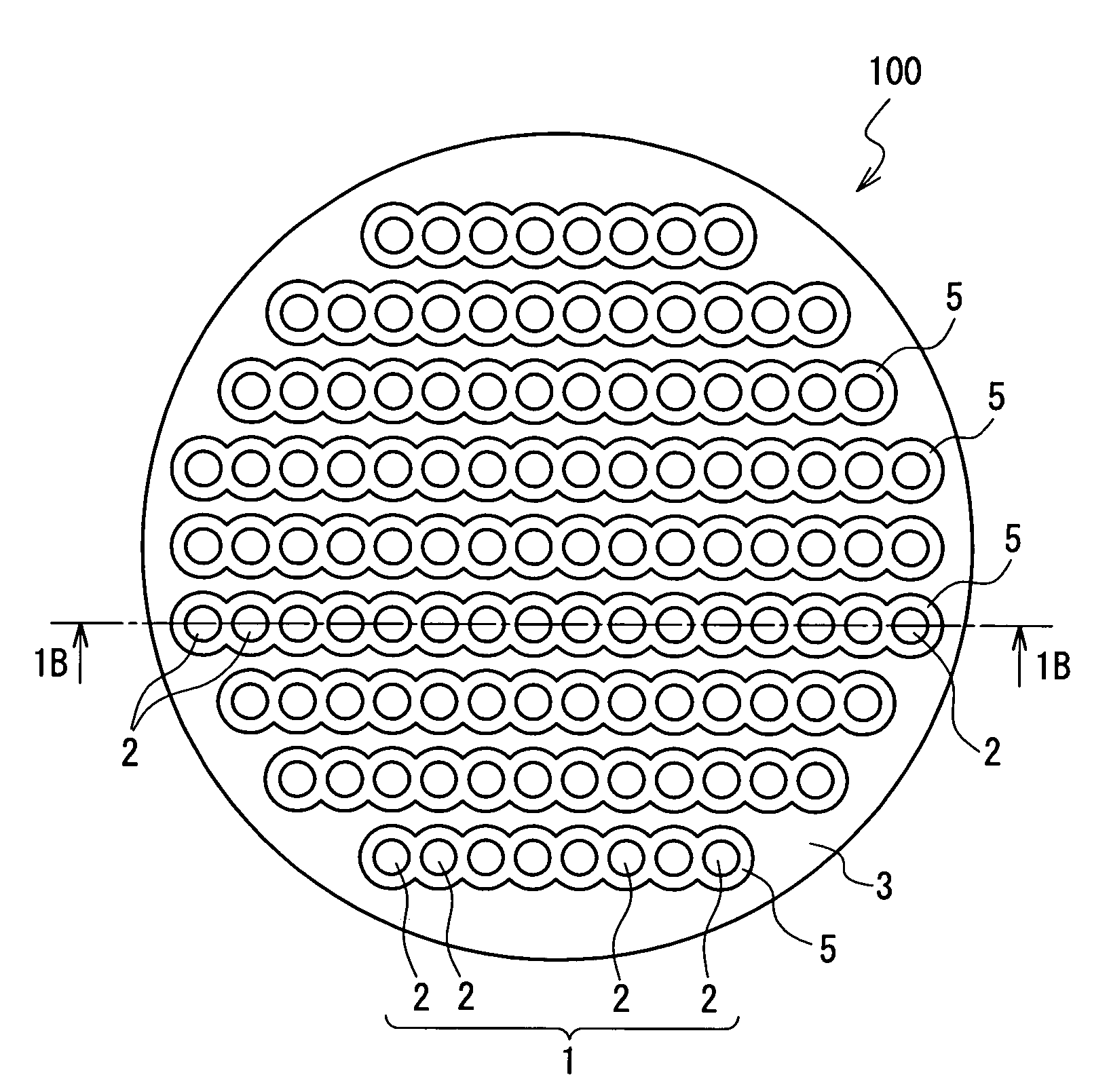
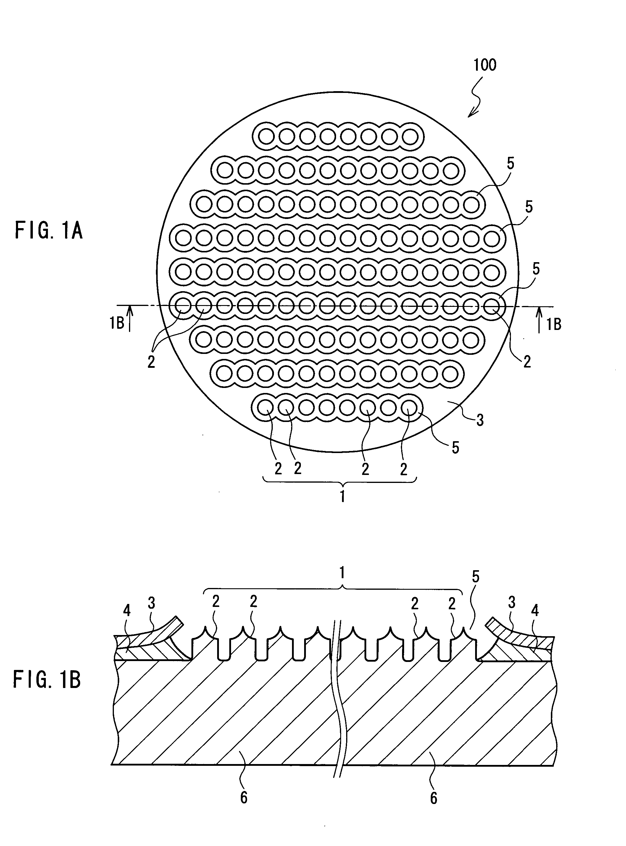
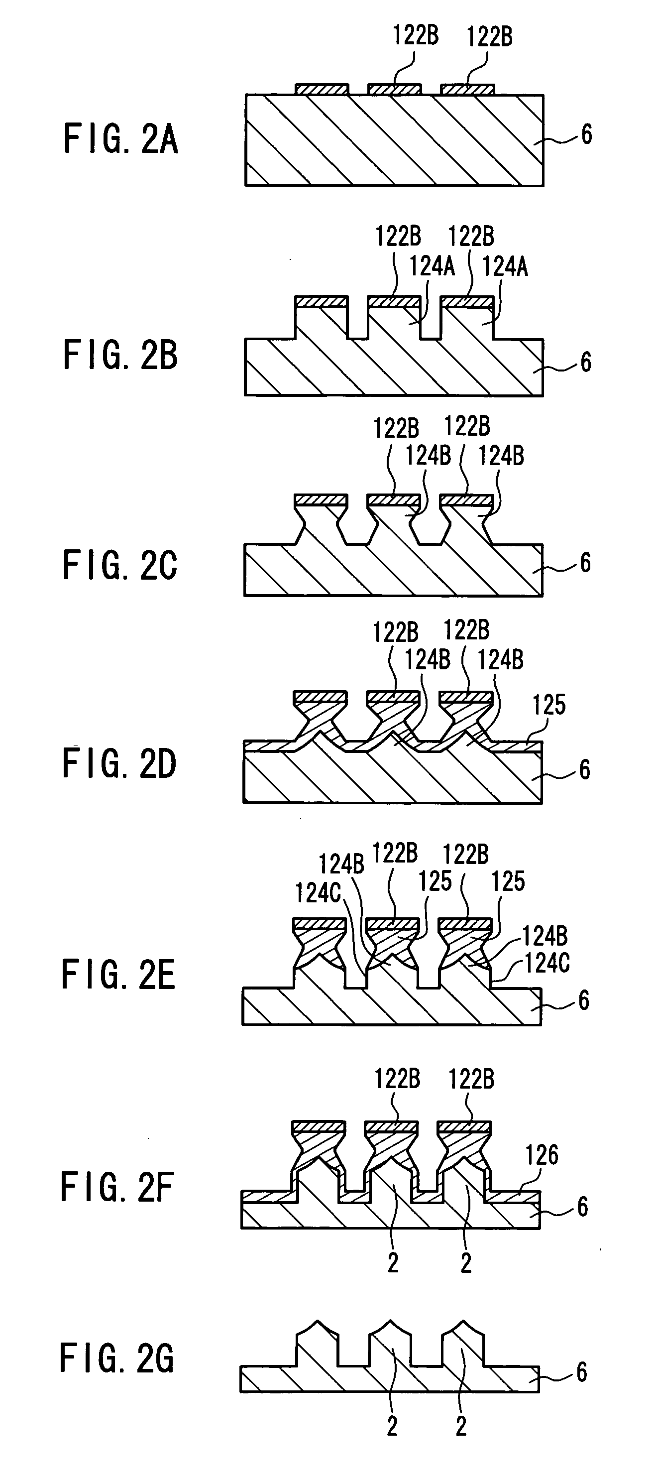
[0060]FIG. 1A is a plan view showing a configuration of a field emission electron source 100 according to Embodiment 1; and FIG. 1B is a cross-sectional view taken on line 1B—1B of FIG. 1A.

[0061]The field emission electron source 100 is provided with a disk-shaped silicon substrate 6. Impurities are introduced in the silicon substrate 6 in order to reduce resistance.

[0062]On the substrate 6, an insulating layer 4 having a plurality of openings 5 each having substantially an elongated-hole shape arranged in parallel with each other at predetermined intervals. On the insulating layer 4, an extraction electrode 3 is formed so that it surrounds the opening 5 of the insulating layer 4.

[0063]In each opening 5, an emitter group 1 is provided. The emitter group 1 includes plurality of emitters 2 aligned in a row along the opening 5 having substantially an elongated opening shape. Each emitter 2 is formed on the surface of the silicon substrate 6. A predetermined voltage is applied to the em...

embodiment 2

[0083]FIG. 3 is a plan view showing a configuration of a field emission electron source 100A according to Embodiment 2. The component elements having the same configurations as the field emission electron source 100 in Embodiment 1 described with the reference to FIGS. 1A and 1B are denoted with the same reference numerals as those therein, and the description thereof will be omitted here.

[0084]In Embodiment 2, a plurality of emitters 2 constituting the emitter group 1A are arranged in two rows so that the two rows are shifted out of registry by a half pitch. Pitch (the relationship between the dot diameter of the micro etching mask and the space between dots) between the emitters 2 constituting the emitter group 1A is the same as shown in Embodiment 1.

[0085]Also in Embodiment 2, it is apparent that open portions 5A of the extraction electrode 3A are formed in a self-aligned manner with respect to the emitter group 1A.

[0086]In Embodiment 2, an electric field to each emitter 2 from t...

embodiment 3

[0087]FIG. 4 is a plan view showing a configuration of a field emission electron source 100B according to Embodiment 3. The component elements having the same configurations as the field emission electron source 100 in Embodiment 1 described with the reference to FIGS. 1A and 1B are denoted with the same reference numerals as those therein, and the description thereof will be omitted here.

[0088]The emitter groups 1B in almost all openings are composed of four emitters 2. Furthermore, in the peripheral region, in order to use an extraction electrode 3B having a circular-shaped periphery more efficiently, some of the emitter groups 1B may be composed of three emitters 2 or may be composed of a single emitter 2. In this way, by designing the number of emitters constituting the emitter group and a method for arranging emitters, etc., in order to arrange the emitters 2 with higher density, a field emission electron source with a large current density can be obtained.

[0089]FIG. 5A is a pl...


PUM


Abstract

A field emission electron source capable of achieving large current density is provided at low cost with good productivity. An insulating layer is formed on a substrate and has one or more openings; and an extraction electrode is formed on the insulating layer. In one or more of the openings, a plurality of emitters, each of which emits an electron by an electric field from the extraction electrode, are formed on the substrate.

Description

FIELD OF THE INVENTION[0001]The present invention relates to a field emission electron source. In particular, it relates to a field emission electron source that is a cold cathode type electron source expected to be applied for a flat-type solid display device or an ultra-speed micro vacuum device and is capable of achieving a large current operation.BACKGROUND OF THE INVENTION[0002]In accordance with the development of fine processing technology of semiconductors, the formation of micro field emission cathodes becomes possible. Spindt et al. proposed a cone type electron emission cathode, so that a micro field emission electron source has drawn attention (reference document 1: C. A. Spindt, J. Appl. Phys. Vol. 39, p. 3504 (1968)).[0003]A structure and manufacturing method of a field emission cathode proposed by Spindt is shown as a first conventional example in FIGS. 11A to 11D.[0004]Referring to FIG. 11A, on the surface of a conductive substrate 101, an insulating layer 102 and a ...

Claims


Application Information

Patent Timeline
Patent Type & Authority Patents(United States)
IPC IPC(8): H01J63/02H01J1/304H01J1/46H01J1/02H01J1/62H01J31/12H01J63/04
CPCH01J1/3044H01J31/127H01J2201/30403
Inventor YAMAMOTO, MAKOTOKOGA, KEISUKESHIOTA, AKINORIKANEMARU, SEIGONAGAO, MASAYOSHI
Owner NAT INST OF ADVANCED IND SCI & TECH
Why Eureka
Try Eureka