GCIB processing of integrated circuit interconnect structures

a technology of integrated circuits and interconnects, applied in the direction of electrical equipment, basic electric elements, electric discharge tubes, etc., can solve the problems of increasing heat dissipation, increasing power consumption, and increasing the difficulty of interconnecting these transistors, so as to improve the fabrication process and quality of metal interconnects, increase device fabrication yields, and extend the usability of current interconnect deposition technologies

Inactive Publication Date: 2006-10-03
TEL EPION
View PDF8 Cites 71 Cited by
  • Summary
  • Abstract
  • Description
  • Claims
  • Application Information

AI Technical Summary

Benefits of technology

[0013]The present invention uses a GCIB to remove and / or redistribute material in the trenches and / or vias of integrated circuit interconnect structures including dual damascene interconnect structures, thereby improving the fabrication process and quality of metal interconnects in an integrated circuit. The process entails opening up or widening the top of a trench or via structure after barrier material and / or seed material deposition in order to allow subsequent thin film deposition and / or filling of the structure, redistributing the barrier and / or seed material from the thicker areas in the trench or via in order to provide a more uniform, continuous thin film coverage of the structure, and / or removing some of the excess and undesired material on the bottom of the structure without significantly damaging or degrading the integrity of the remaining material. The GCIB process may be applied after the barrier metal deposition and before the copper seed layer / copper electroplating or the process may be applied after the formation of the copper seed layer and before copper electroplating.
[0014]The present invention reduces the voids present in the metal interconnect lines and / or contact vias, increases the device fabrication yields, and allows for the recovery of failed devices thereby extending the usability of the current interconnect deposition technologies to the next generation integrated circuits and beyond.

Problems solved by technology

The challenge to interconnect these transistors becomes increasingly difficult.
Some of the problems faced with denser interconnections are increased heat dissipation, greater power consumption, and longer signal delays resulting from higher resistance in the interconnects.
One of the difficulties with fabricating such high aspect ratio interconnect structures is the barrier material, which is employed to encapsulate the metal conductor to prevent diffusion into the surrounding semiconductor materials, must be deposited in such a way as to form a continuous layer on the sidewalls of the trenches and vias.
Depositing these barrier materials and copper seed layers into high aspect ratio, sub-quarter micron vias and trenches often result in uneven thicknesses at the top of the structure, on the side walls and on the bottom of the structure.
These effects result in at least three distinct problems that negatively influence the performance of the semiconductor device.
First, an excessive overhang of material at the top of the trench or via may cause a “necking in” of the opening which may restrict or prohibit subsequent thin film depositions and / or filling of the structure with the interconnect metal.
This problem may then result in voids in the interconnect metal and thus failed devices.
Second, a poor sidewall coverage, especially near the bottom corners of the structure, results in too thin of a barrier material layer to prevent copper diffusion and / or too thin of a copper seed layer to allow subsequent copper electroplating and thus failed devices.
Third, a build up of material at the bottom of the trenches or vias due to excessive barrier thin film deposition may cause the structures to have substantially higher intrinsic resistivities (typically 100–1000 micro-Ohm-cm) compared to the interconnect metals (1.7 to 3.5 micro-Ohm-cm).
This problem results in a significantly higher contact resistance for the interconnect metal and thus negatively influences the performance / speed of the device.
Consequently, the impact effects of large clusters are substantial, but are limited to a very shallow surface region.

Method used


Image

  • GCIB processing of integrated circuit interconnect structures
  • GCIB processing of integrated circuit interconnect structures
  • GCIB processing of integrated circuit interconnect structures

Examples


Embodiment Construction

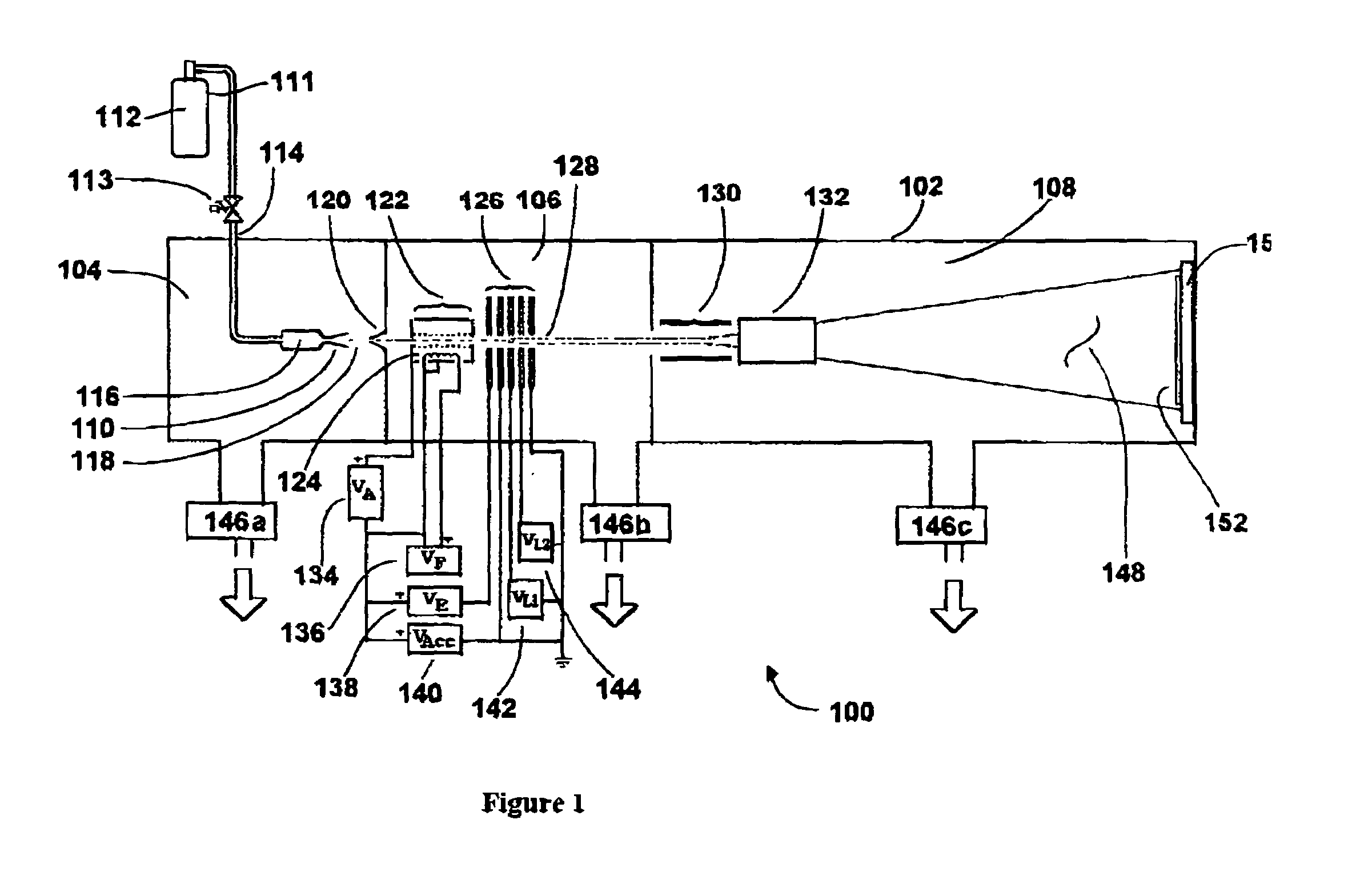
[0024]FIG. 1 shows a schematic of the basic elements of a typical configuration for a GCIB processor 100 of a form known in prior art, and which may be described as follows: a vacuum vessel 102 is divided into three communicating chambers, a source chamber 104, an ionization / acceleration chamber 106, and a processing chamber 108. The three chambers are evacuated to suitable operating pressures by vacuum pumping systems 146a, 146b, and 146c, respectively. A condensable source gas 112 (for example argon or N2) stored in a gas storage cylinder 111 is admitted under pressure through gas metering valve 113 and gas feed tube 114 into stagnation chamber 116 and is ejected into the substantially lower pressure vacuum through a properly shaped nozzle 110. A supersonic gas jet 118 results. Cooling, which results from the expansion in the jet, causes a portion of the gas jet 118 to condense into clusters, each consisting of from several to several thousand weakly bound atoms or molecules. A ga...


PUM

PropertyMeasurementUnit
energyaaaaaaaaaa
angleaaaaaaaaaa
pressureaaaaaaaaaa

Abstract

Method for removing and / or redistributing material in the trenches and / or vias of integrated circuit interconnect structures by a gas cluster ion beam (GCIB) is described to improve the fabrication process and quality of metal interconnects in an integrated circuit. The process entails opening up an undesired ‘necked in’ region at the entrance to the structure, re-depositing the barrier metal from thicker areas such as the neck or bottom of the structure to the side walls and / or removing some of the excess and undesired material on the bottom of the structure by sputtering. The GCIB process may be applied after the barrier metal deposition and before the copper seed layer / copper electroplating or the process may be applied after the formation of the copper seed layer and before electroplating. The method may extend the usability of the known interconnect deposition technologies to next generation integrated circuits and beyond.

Description

CROSS-REFERENCE TO RELATED APPLICATIONS[0001]This application claims the benefit of priority to U.S. Provisional Application Ser. No. 60 / 424,967 filed Nov. 8, 2002, and entitled “GCIB Processing Of Dual Damascene Structures”, the contents of which are hereby incorporated by reference.FIELD OF THE INVENTION[0002]This invention relates generally to applying gas cluster ion beams (GCIB) to integrated circuit interconnect structures in order to improve the fabrication process and quality of metal interconnects in an integrated circuit, and, more particularly to improve the process and quality by removing and / or redistributing material in the trenches and / or vias of integrated circuit interconnect structures, including dual damascene interconnect structures.BACKGROUND OF THE INVENTION[0003]In the semiconductor industry, increasing circuit density drives progress toward smaller and smaller dimensions and larger numbers of transistors placed in an individual device. The challenge to interc...

Claims


Application Information

Patent Timeline
Patent Type & Authority Patents(United States)
IPC IPC(8): H01L21/302C23F4/00H01LH01L21/3213H01L21/768
CPCC23F4/00H01L21/32135H01L21/76843H01L21/76862H01L21/76865H01L21/76877H01J2237/0812
Inventor HAUTALA, JOHN J.
Owner TEL EPION
Why Eureka
Try Eureka