DC-DC converter

a converter and dc technology, applied in the field of dc converters, can solve problems such as increasing switching losses

Active Publication Date: 2006-10-03
TEXAS INSTR INC +1
View PDF9 Cites 45 Cited by
  • Summary
  • Abstract
  • Description
  • Claims
  • Application Information

AI Technical Summary

Benefits of technology

[0007]The purpose of the present invention is to solve the aforementioned problems of the aforementioned conventional technology by providing a DC—DC converter that can reduce the peak value of the current flowing through the inductance element and that can suppress the ripple in the output current.
[0009]In the aforementioned configuration, in the first state, one of the terminals of the inductance element is connected to the ground potential via the second switching element in the on state, and the other terminal of the inductance element is connected to the voltage output terminal via the third switching element in the on state. Energy is released from the inductance element to the voltage output terminal, and the current flowing through the inductance element (coil current) falls at a certain steep slope or decreases over time. In the second state, one of the terminals of the inductance element is connected to the voltage input terminal via the first switching element in the on state, and the other terminal of the inductance element is connected to the ground potential via the fourth switching element in the on state. Energy from the voltage input terminal is stored in the inductance element, and the coil current rises at a certain steep slope or increases over time. In the third state, one of the terminals of the inductance element is connected to the voltage input terminal via the first switching element in the on state, and the other terminal of the inductance element is connected to the voltage output terminal via the third switching element in the on state. Energy is released from the inductance element to the voltage output terminal while the energy from the voltage input terminal is stored in the inductance element. The coil current stays at an almost constant level immediately after switching if the input and output voltages are close to each other, and rises or falls at a slope corresponding to the ratio of magnitudes if the input and output voltages are significantly different from each other. In the fourth state, one of the terminals of the inductance element is connected to the ground potential via the second switching element in the one state, while the other terminal of the inductance element is connected to the ground potential via the fourth switching element in the on state. The coil current stays at an almost constant level immediately after the switching, irrespective of the ratio of magnitudes between the input and output voltages. When the aforementioned first, second, third, and fourth states are repeated, in particular, when the fourth state is included in one cycle, the variation or peak level of the coil current can be reduced. When the peak level of the coil current is reduced, the ripple in the output voltage can also be reduced.
[0010]According to a preferable embodiment of the present invention, the four states are repeated in an order such that the fourth state comes after the aforementioned third state with one state, either the first or the second state, inserted between them, and the third state comes after the fourth state with the other state, either the first or the second state, inserted between them. In this case, since the first state, in which the coil current drops sharply, and the second state, in which the coil current rises sharply, are not arranged in succession, in particular, since the fourth state, in which the coil current stays almost unchanged unconditionally, is inserted between the first and second states, the deflection point or the peak level of the coil current is effectively dulled or suppressed, and the peak level can be further reduced.
[0011]In the present invention, the variation or peak level of the coil current can be reduced if the period of the third and fourth states is longer than the period of the first and second states.
[0018]According to yet another preferred embodiment of the present invention, the maximum peak point and the minimum peak point of the first triangular signal occur at the same time or close to the maximum peak point and the minimum peak point of the second triangular signal on the time axis, respectively, and the switching is controlled in the following way. When the voltage level of the aforementioned feed forward signal is higher than the voltage level of the first triangular signal, the first switching element is off and the second switching element is on. When the voltage level of the aforementioned feed forward signal is lower than the voltage level of the first triangular signal, the first switching element is on and the second switching element is off. When the voltage level of the aforementioned feed forward signal is higher than the voltage level of the second triangular signal, the third switching element is off and the fourth switching element is on. When voltage level of the aforementioned feed forward signal is lower than the voltage level of the second triangular signal, the third switching element is on and the fourth switching element is off. In this way, the first, second, third, and fourth states can be repeated in a preferred order.
[0019]According to yet another preferred embodiment of the present invention, the maximum peak point and the minimum peak point of the first triangular signal occur at the same time or close to the maximum peak point and the minimum peak point of the second triangular signal on the time axis, respectively, and the switching is controlled in the following way. When the voltage level of the aforementioned feed forward signal is higher than the voltage level of the first triangular signal, the first switching element is on and the second switching element is off. When the voltage level of the aforementioned feed forward signal is lower than the voltage level of the first triangular signal, the first switching element is off and the second switching element is on. When the voltage level of the aforementioned feed forward signal is higher than the voltage level of the second triangular signal, the third switching element is on and the fourth switching element is off. When voltage level of the aforementioned feed forward signal is lower than the voltage level of the second triangular signal, the third switching element is off and the fourth switching element is on. In this way, the first, second, third, and fourth states can be repeated in a preferred order.

Problems solved by technology

Also, a larger peak value of the coil current requires the use of an inductance element with larger rated current (that is, larger size), which also increases switching loss.

Method used


Image

  • DC-DC converter
  • DC-DC converter
  • DC-DC converter

Examples


embodiment 1

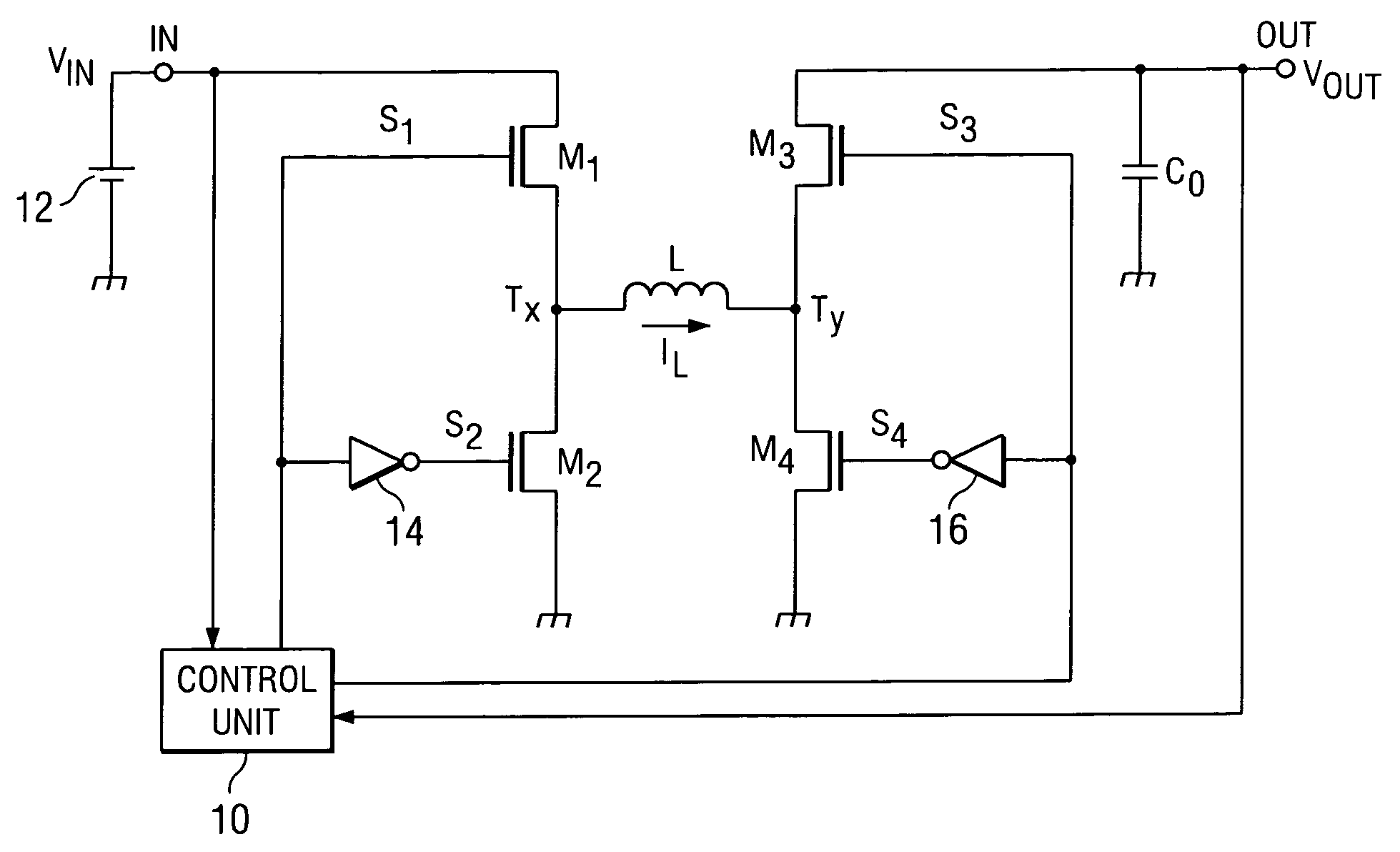
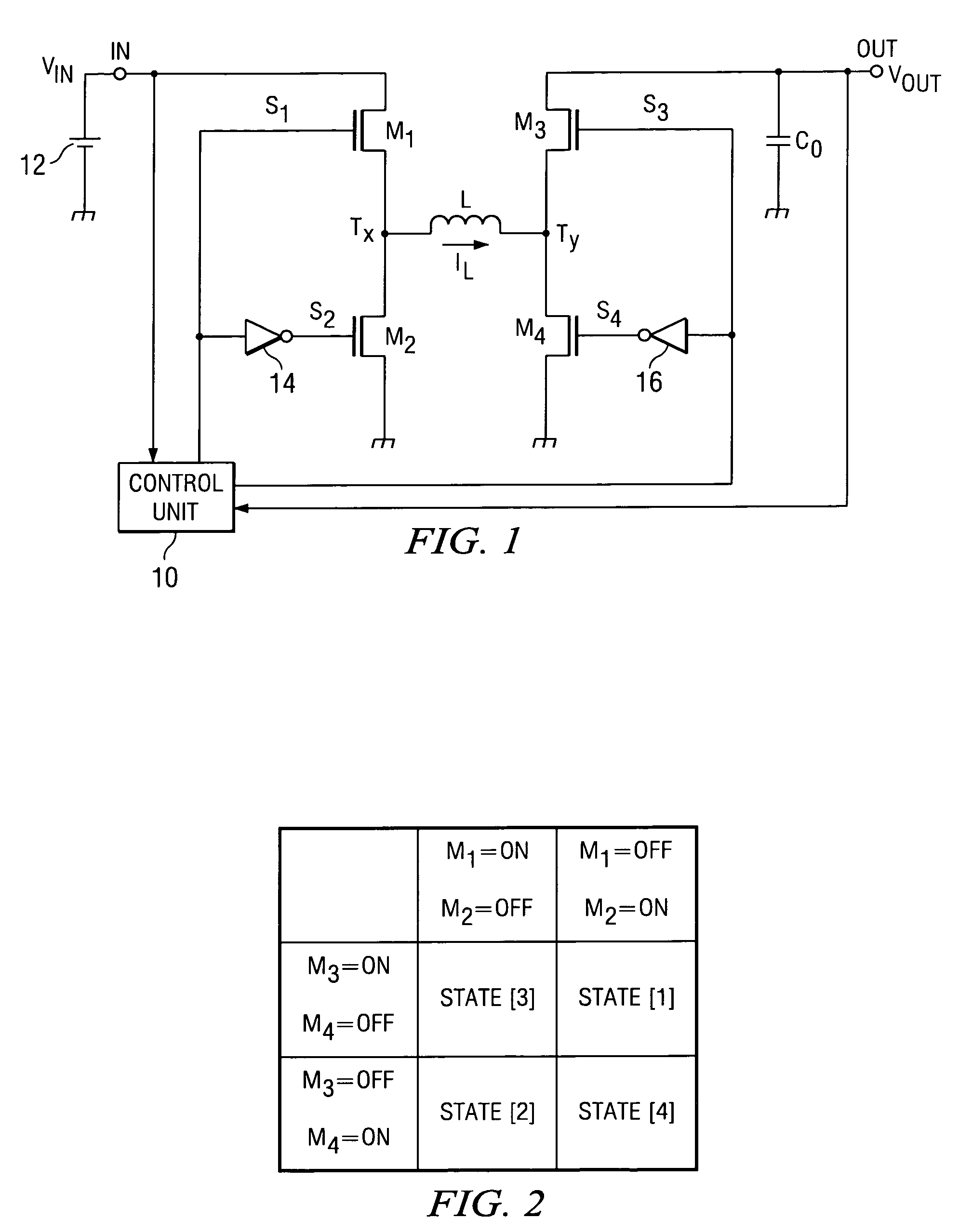
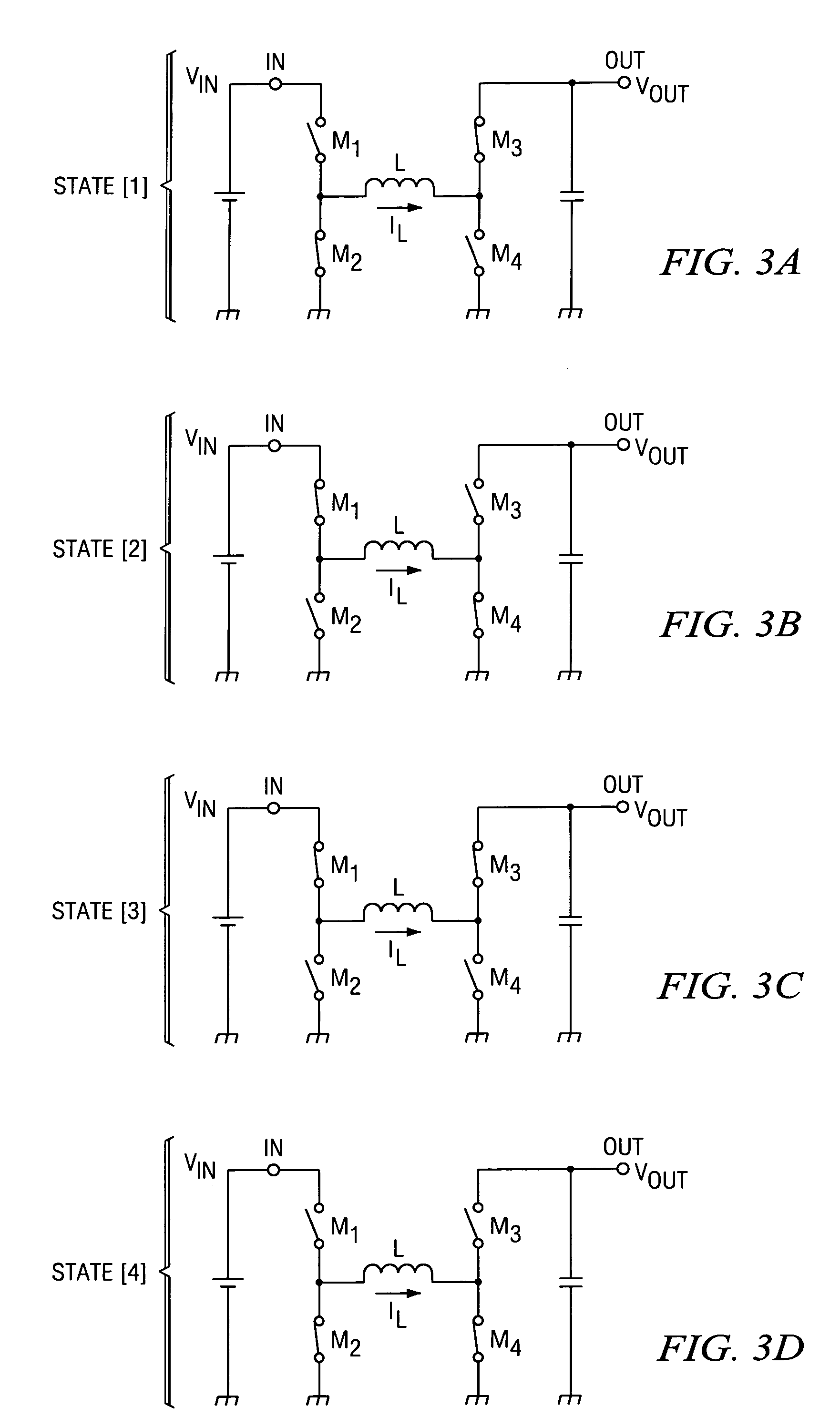
[0047]FIG. 6 shows the circuit configuration of the step-up / step-down DC—DC converter disclosed in the first embodiment.

[0048]In this DC—DC converter, control unit 10 has feed forward control circuit 18 on the side of switching elements M1, M2 and feedback control circuit 20 on the side of switching elements M3, M4.

[0049]Feed forward control circuit 18 has input voltage monitoring circuit 30, PWM (pulse width modulation) comparator 32, and triangular signal generating circuit 34. In this case, input voltage monitoring circuit 30 has voltage-dividing resistor circuit 22, operational amplifier 24, feedback resistor 26, and reference voltage generating circuit 28. In input voltage monitoring circuit 30, coefficient Ka determined by the voltage-dividing ratio of the voltage-dividing resistor circuit 22 and the resistance of feedback resistor 26 is multiplied with the input voltage Vin, and this multiplication result is added to constant D corresponding to the reference voltage Vref gene...

embodiment 2

[0066]FIG. 11 shows the circuit configuration of the step-up / step-down type DC—DC converter disclosed in the second embodiment. In the second embodiment, in the aforementioned DC—DC converter (FIG. 6) described in the first embodiment, inverted triangular signal generating circuit 48 is omitted, and the same triangular signal Wa as that applied to PWM comparator 32 on the side of feedforward control circuit 18 is applied to PWM comparator 46 on the side of feedback control circuit 20. However, triangular signal Wa is input to input terminal (+) of PWM comparator 46, while the feedback error signal Vb from error signal detecting circuit 44 is input to the other input terminal (−). Consequently, comparator 46 compares the voltage level of feedback error signal Vb with the voltage level of triangular signal Wa. If Vb>Wb, an output voltage, that is, control signal S3 with level L is output. If Vb3 with level H is output. The rest of the configuration is exactly the same as that describe...


PUM


Abstract

The objective of this invention is to reduce the current flowing through the inductance element in a step-up / step-down DC—DC converter and to control the ripple in the output voltage. In the DC—DC converter, four states, that is, the first state [1] of (M1, M2)=(off, on) and (M3, M4)=(on, off), the second state [2] of (M1, M2)=(on, off) and (M3, M4)=(off, on), the third state [3] of (M1, M2)=(on, off) and (M3, M4)=(on, off), and the fourth state [4] of (M1, M2)=(off, on) and (M3, M4)=(off, on) are repeated in a prescribed order, preferably in the order . . . [1]→[4]→[2]→[3]→[1] . . . or . . . [1]→[3]→[2]→[4]→[1] . . . .

Description

CROSS REFERENCE TO RELATED APPLICATIONS[0001]This application claims priority under 35 USC § 119 of Japanese Application Serial No. 2003-429,254, filed Dec. 25, 2003.FIELD OF THE INVENTION[0002]The present invention pertains to a DC—DC converter used to convert an input DC (direct current) power to a different DC (direct current) power.[0003]DC—DC converters are small, light, and highly efficient DC power supplies using semiconductor switching elements. They are widely used for electronic devices, etc. In recent years, there has been a strong demand for smaller size, lighter weight, and higher efficiency. The basic working theory of DC—DC converters is that the switching elements are turned on / off at high frequency, and the ratio of the on time and off time, that is, the duty ratio, is controlled in a variable manner to keep the DC output voltage at a certain level. The so-called non-isolating or chopper type DC—DC converters can be classified into 3 types, that is, the step-up type...

Claims


Application Information

Patent Timeline
Patent Type & Authority Patents(United States)
IPC IPC(8): G05F1/613H02M3/155H02M1/15H02M3/158H02M3/335
CPCH02M1/15H02M3/1582
Inventor IKEZAWA, KATSUYA
Owner TEXAS INSTR INC
Why Eureka
Try Eureka