Resource board for emulation system

a technology of emulation system and resource board, which is applied in the direction of error detection/correction, program control, instruments, etc., can solve the problems of not providing any assurance that the new and old portions of the design will work properly together, requiring a lot of processing time to simulate ic behavior, and the hard-wired approach to fpga interconnection is relatively inexpensive, and not very flexibl

Active Publication Date: 2006-10-10
SYNOPSYS INC
View PDF13 Cites 18 Cited by
  • Summary
  • Abstract
  • Description
  • Claims
  • Application Information

AI Technical Summary

Benefits of technology

[0018]When a workstation is to emulate a portion of the IC, the packet routing network can also provide virtual signal paths between the workstation and the resource boards. The workstation can also send PLD programming data via packets to the network / resource interface circuit on each resource board, with each packet being addressed to a particular PLD to be programmed. A “select map” bus connected between the network / resource interface circuit and each PLD on the board allows the network / resource interface circuit to forward programming data arriving in a packet to the addressed PLD. Thus an emulation resource board in accordance with the invention provides a convenient way to interface a workstation to emulation resources on the board to allow the workstation to program the emulation resources on the board and to also emulate a portion of the IC being emulated and to program the emulation resources on the board.
[0019]A resource board in accordance with a preferred embodiment of the invention includes several FPGAs or other types of PLDs and a separate random access memory (RAM) corresponding to each FPGA. A set of switches controlled by the network / resource interface circuit in response to control data received via incoming packets selectively couple terminals of each FPGA to its corresponding RAM, thereby allowing circuits emulated by the FPGA to read and write access the RAM so that the RAM can emulate memory embedded in the circuit being emulated.
[0023]Thus an emulation resource board in accordance with the invention holds PLDs and RAMs and employs both hard-wired and virtual signal paths to flexibly route signals between the PLDs and RAMS on the resource board and between the PLDs and other resource boards, workstations and other external equipment. The resource board also provides the logic and balanced signal paths needed to deliver clock signals to the PLDs and reduces the number of signals needed to communicate with external test equipment by implementing much of the pattern generation and data acquisition functionality needed to test an emulated circuit.

Problems solved by technology

Although a simulator can accurately model the behavior of an IC based on either a high-level or gate-level netlist, it can require much processing time to simulate IC behavior.
To reduce simulation time a designer can program a simulator to simulate only selected portions of an IC design that are new or have been modified, but this approach may not provide any assurance that the new and old portions of the design will work properly together.
This hard-wired approach to FPGA interconnects is relatively inexpensive, but not very flexible since the number of direct signal paths between each pair of FPGA 14, and between the resource board and other resource boards or test equipment is fixed.
In cases where there are no direct signal paths between two FPGAs 14 that are to communicate with one another, or for which there are an insufficient number of direct signals paths, additional signals can be routed through interposing FPGAs, however in such case some of the FPGA resources will be expended on signal routing duties and be unavailable for logic emulation.
But since the number of signal paths switch matrix 34 must provide is proportional to the square of the number of FPGA terminals and buffered signal paths to be interconnected, the necessary switch matrix size becomes impractically large for a circuit board having a large array of FPGAs, each having a large number of IO terminals.

Method used


Image

  • Resource board for emulation system
  • Resource board for emulation system
  • Resource board for emulation system

Examples


Embodiment Construction

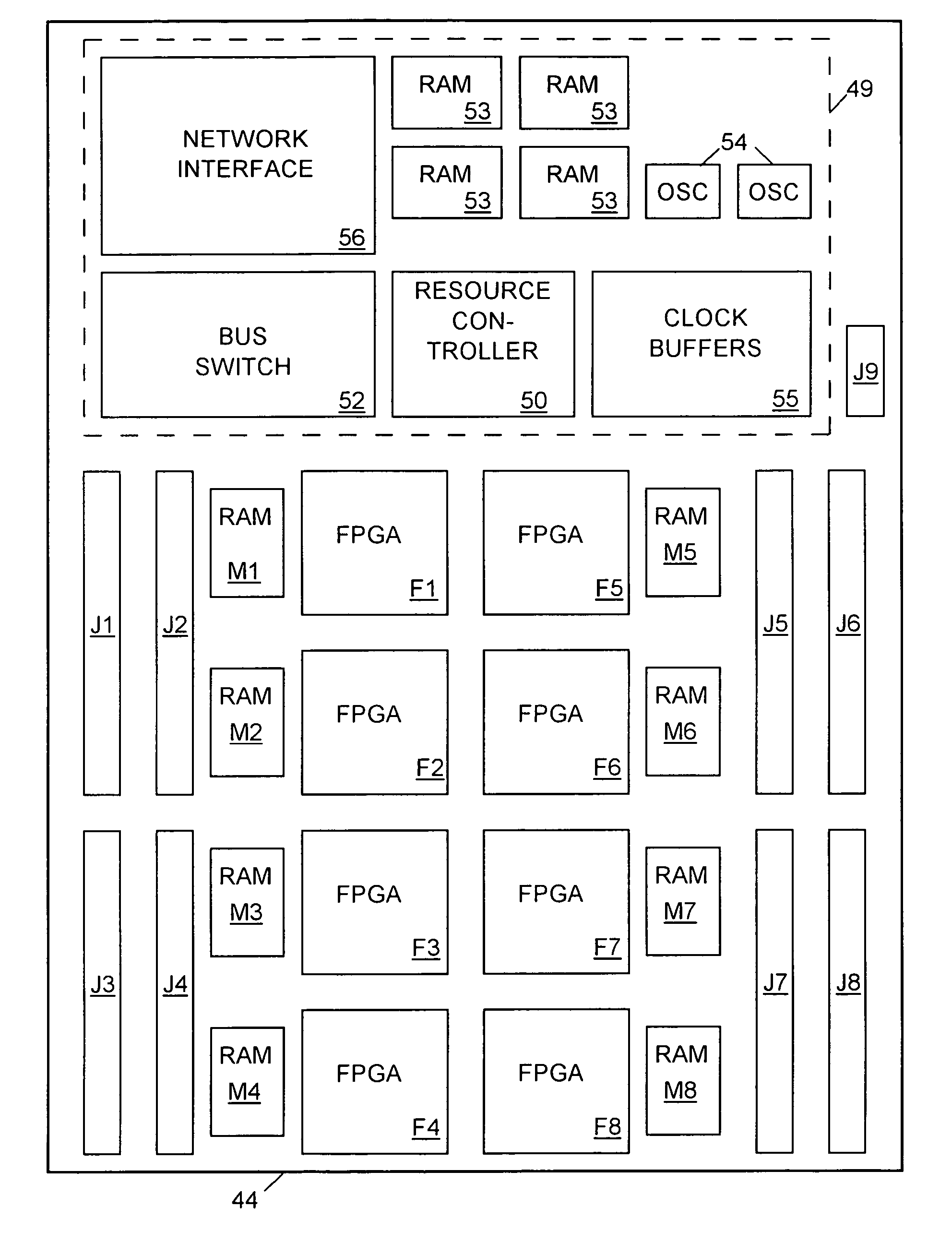
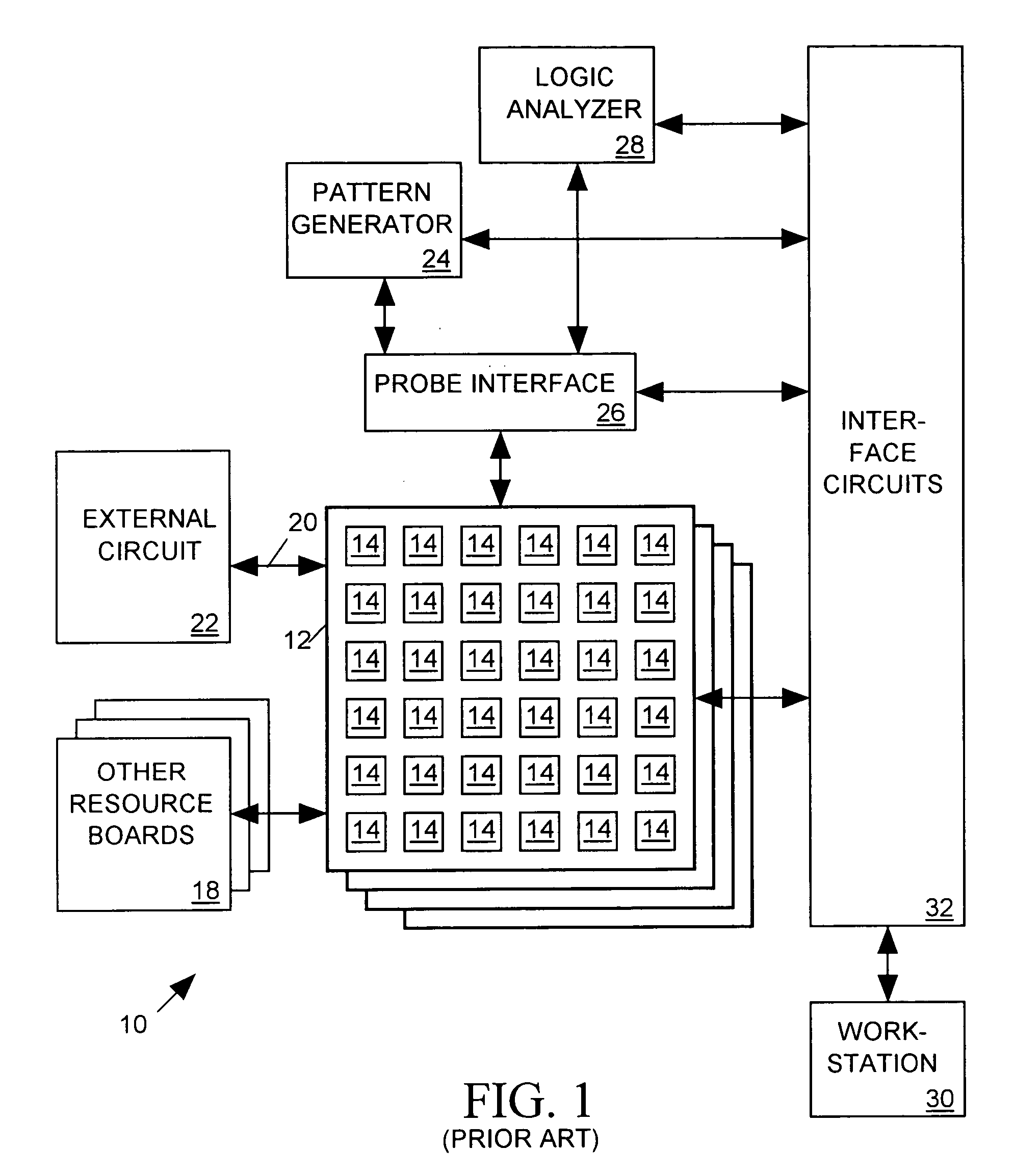
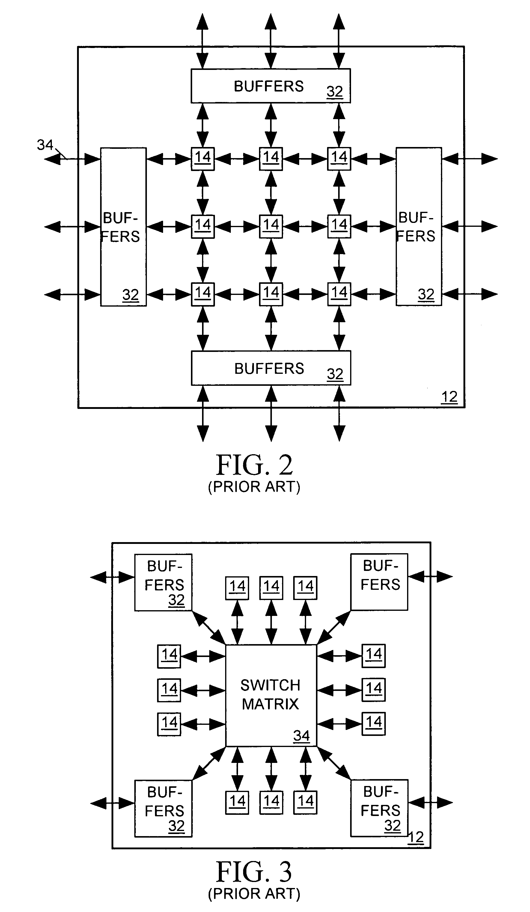
[0031]The present invention relates to a network-based emulation system using various programmable resources to emulate the behavior of an IC to determine how signals an IC produces would behave in response to test signals applied as inputs to the IC. The invention relates in particular to a circuit board employed by the emulation system for holding emulation resources, for providing programming and data signal paths to the resources, and for providing some test functions needed during a circuit emulation. While the specification below and the accompanying drawings depict an example embodiment of an emulation resource board considered to be a best mode of practicing the invention, those of skill in the art will appreciate that the invention may be practiced in other ways. The claims appended to this specification therefore apply not only to the example embodiment described below but to any embodiment of the invention including elements or steps that may be functional equivalents of ...


PUM


Abstract

A resource board for a circuit emulator holds programmable logic devices (PLDs) and other emulation resources such as random access memories (RAMs) and employs both hard-wired and network-based virtual signal paths to flexibly route signals between the emulation resources on the resource board and resources mounted on other resource boards, workstations and other external equipment. The resource board also provides the logic and balanced signal paths needed to deliver clock signals to the PLDs and reduces the number of signals needed to communicate with external test equipment by implementing much of the pattern generation and data acquisition functionality needed to test an emulated circuit.

Description

CROSS-REFERENCE TO RELATED APPLICATIONS[0001]The present application is a continuation-in-part of copending application Ser. No. 10 / 463,057 filed Jun. 16, 2003 and incorporated herein by reference.BACKGROUND OF THE INVENTION[0002]1. Field of the Invention[0003]The present invention relates to systems employing programmable logic devices and other resources to emulate the behavior of an electronic circuit, and in particular to a circuit board for providing emulation resources for an emulation system.[0004]2. Description of Related Art[0005]A typical digital integrated circuit (IC) employs register transfer logic (RTL) wherein each block of logic within the IC includes an output register for synchronizing state changes in its output signals to edges of a clock signal. An IC designer will usually generate an initial, high-level netlist employing Boolean expressions to characterize each block of logic. The designer will then employ a synthesis tool to convert the high level netlist into...

Claims


Application Information

Patent Timeline
Patent Type & Authority Patents(United States)
IPC IPC(8): G06F9/455G06F17/50G06F11/22G06F11/26G06F17/00H01L21/82
CPCG06F11/261G06F17/5027G06F30/331
Inventor SHEI, SWEYYANWANG, MING YANGCHIU, VINCENTNGUI, NEU CHOO
Owner SYNOPSYS INC
Why Eureka
Try Eureka