
Semiconductor device and method of manufacturing the same

a semiconductor and semiconductor technology, applied in the field of semiconductor devices, can solve the problems of difficult to raise the degree of integration in the wiring layer, difficult to reduce the width of the peripheral circuit region, and higher than ideal resistance of the wiring, so as to improve the aperture ratio of the pixel region, reduce the area of the peripheral circuit region, and reduce the width

Inactive Publication Date: 2006-10-17
SEMICON ENERGY LAB CO LTD +1
View PDF9 Cites 36 Cited by
  • Summary
  • Abstract
  • Description
  • Claims
  • Application Information

AI Technical Summary

Benefits of technology

[0012]The present invention has been made in view of the above circumstances, and an object of the present invention is therefore to provide a technique for reducing the area of a peripheral circuit region with respect to a pixel region. In particular, an object of the present invention is to improve the aperture ratio of the pixel region by giving the peripheral circuit region (“border frame”) a smaller width through a multilayer wiring.
[0017]According to the above semiconductor device, the wiring in the peripheral circuit region is formed from a low resistance material, thereby giving the wiring a smaller width. Therefore, the area of the peripheral circuit region with respect to the area of the pixel region can be reduced.
[0023]According to the above semiconductor device, the wiring formed in the peripheral circuit region is a multilayer wiring and therefore the peripheral circuit region (border frame) is given a smaller width. In this way, the pixel region can have an improved aperture ratio.
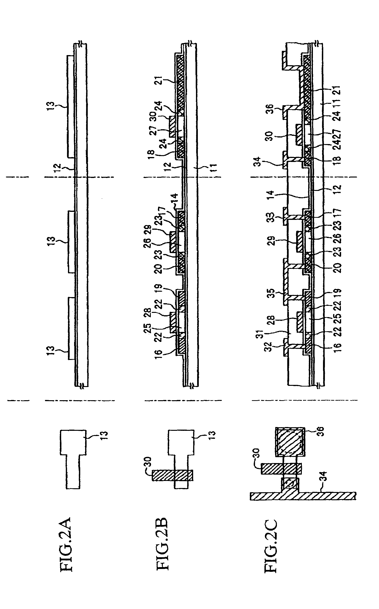
[0056]According to the above method of manufacturing a semiconductor device, the first through third wirings are formed over the driver circuit TFT and the first and second capacitor elements are formed on the drain region of the pixel TFT. Therefore, the pixel region can have an improved aperture ratio.

Problems solved by technology

In the conventional liquid crystal display device described above, the wiring layer is a single layer and raising the degree of integration in the wiring layer is difficult due to limitations of a photolithography system or the like.
When wirings are formed in the same layer, the wirings take up a large area and the proportion of the area of the driver circuit and other peripheral circuits to the entire chip area is accordingly large, presenting an obstacle to reduction in width of the peripheral circuit region.
This could result in higher-than-ideal resistance for the wirings and a shortage of current to be supplied to the TFTs.
This could result in level discontinuity in the wirings patterned.

Method used


Image

  • Semiconductor device and method of manufacturing the same
  • Semiconductor device and method of manufacturing the same
  • Semiconductor device and method of manufacturing the same

Examples


embodiment mode 1

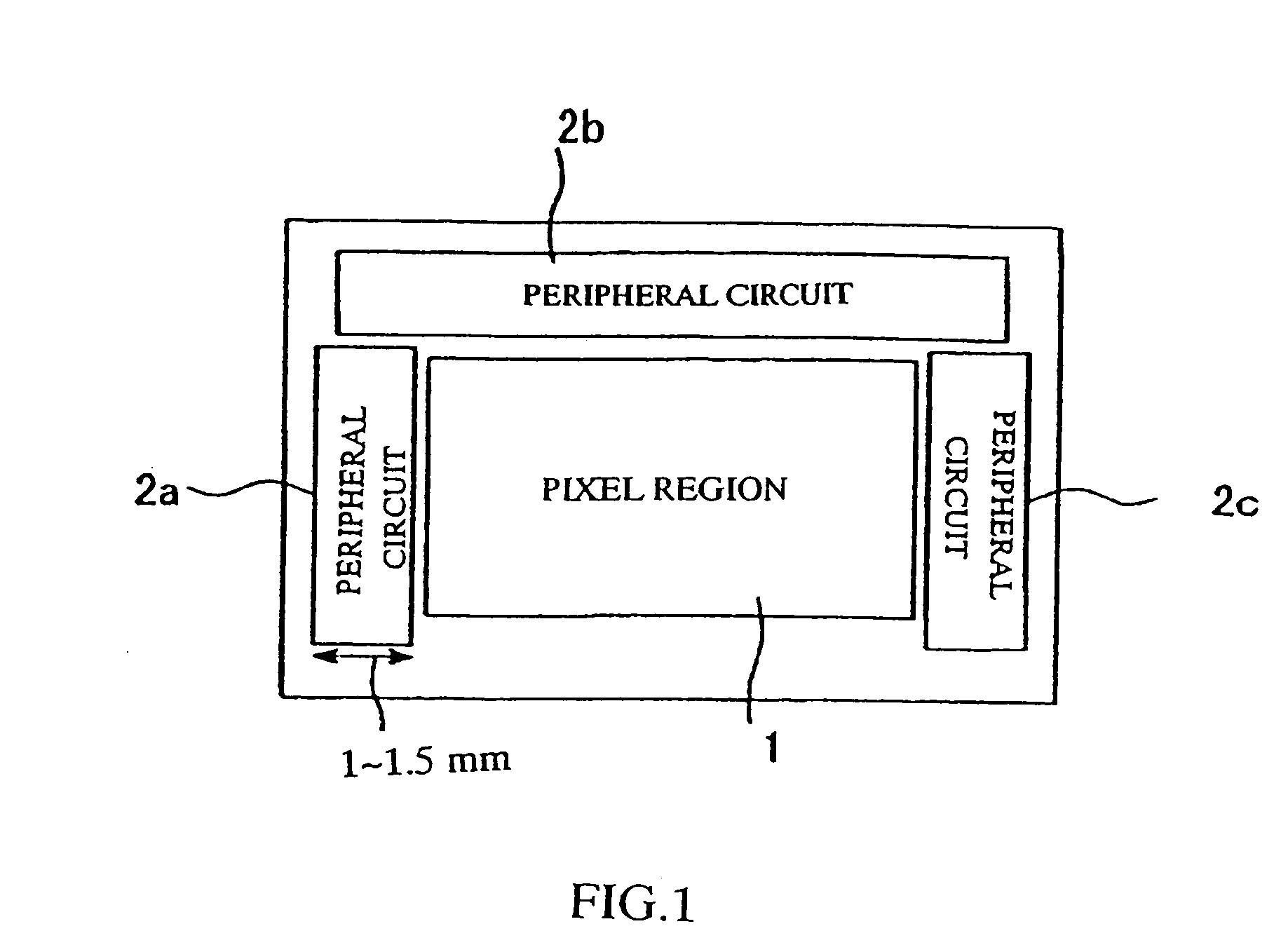
[0109]FIG. 1 is a plan view schematically showing a chip in a liquid crystal display device of Embodiment Mode 1 according to the present invention.

[0110]This chip in the liquid crystal display device has a pixel region 1, which has a substantially square shape in plan view. The pixel region 1 is composed of one or more pixels. Placed in the periphery (above, to the left, and to the right) of the pixel region 1 are peripheral circuits 2a to 2c. Chips like this are arranged on a substrate. The peripheral circuits 2a to 2c each have a substantially thin rectangular shape in plan view, and the shorter sides of each rectangular are 1 to 1.5 mm in length. The peripheral circuits 2a to 2c therefore have a smaller width than in conventional liquid crystal display devices.

[0111]In order to give the peripheral circuits a smaller width and reduce the area of the peripheral circuit region (border frame) with respect to the area of the pixel region to improve the aperture ratio, methods describ...

embodiment mode 2

[0119]Described next is a liquid crystal display device according to Embodiment Mode 2 of the present invention.

[0120]In this embodiment mode, gate electrodes of TFTs are formed isolatedly from one another. In other words, a gate electrode in a TFT and a gate electrode in another TFT are formed separately. This means that, instead of leading a wiring which is in the same layer as a gate electrode and which is connected to the gate electrode, a wiring formed in an upper or lower layer of a gate electrode is electrically connected to the gate electrode and led. This eliminates the need to lower the resistance of the gate electrode and makes it possible to thin the gate electrode. An example of the lower layer wiring is a wiring interposed between a substrate and a Si active layer. Materials that are employable for the gate electrode are N+ polysilicon and a refractory metal the same as in prior art. By thus thinning the gate electrode, level differences caused by the thickness of the ...

embodiment mode 3

[0121]Next, a description is given on a liquid crystal display device according to Embodiment Mode 3 of the present invention.

[0122]In this embodiment mode, a gate electrode is only given the function of a gate electrode and formed not to have the function of a wiring by isolating a gate electrode in one TFT from a gate electrode in another TFT. A wiring is formed in an upper or lower layer of a gate electrode and is electrically connected to the gate electrode to give the wiring the wiring function of the gate electrode in prior art as well as the function of a short distance wiring, one of the wirings of prior art that has a short wiring length. Similar to Embodiment Mode 2, an example of the lower layer wiring is a wiring interposed between a substrate and a Si active layer.

[0123]As described, by taking the wiring function away from the gate electrode of prior art and giving this function to a wiring in a layer above the gate electrode, this embodiment mode makes it possible to u...


PUM

PropertyMeasurementUnit
lengthaaaaaaaaaa
widthaaaaaaaaaa
distanceaaaaaaaaaa

Abstract

The present invention provides a semiconductor device wherein the area of a peripheral circuit region with respect to a pixel region is reduced, and provides a manufacturing method of the semiconductor device. A semiconductor device according to the present invention is characterized by having a pixel region 1, peripheral circuit regions 2a to 2c arranged in at least a part of the periphery of the pixel region, and a wiring formed in the peripheral circuit region, and by having a wiring multilayered with two or more layers. At least one layer of the multilyered wiring is formed from a low resistance material. Transistors are formed in the peripheral circuit region, and the multilayer wiring with two or more layers is formed on the upper side of the transistors.

Description

BACKGROUND OF THE INVENTION[0001]1. Field of the Invention[0002]The present invention relates to a semiconductor device and a method of manufacturing the semiconductor device, and more specifically to a technique of reducing the area of a peripheral circuit region with respect to a pixel region that has one or more pixels. The present invention also relates to a technique of improving an aperture ratio of the pixel region by giving the peripheral circuit region (“border frame”) a smaller width through a multilayer wiring.[0003]2. Description of the Related Art[0004]FIG. 6 is a plan view schematically showing a chip in a conventional liquid crystal display device.[0005]This chip in the liquid crystal display device has a pixel region 101, which has a square shape in plan view. The pixel region 101 is composed of one or more pixels. Placed in the periphery (above, to the left, and to the right) of the pixel region 101 are peripheral circuits 102a to 102c. The chip is arranged on a sub...

Claims


Application Information

Patent Timeline
Patent Type & Authority Patents(United States)
IPC IPC(8): H01L29/04H01L29/15G02F1/1368G02F1/1345G02F1/1362H01L21/3205H01L21/768H01L21/77H01L21/84H01L23/52H01L27/12H01L29/786
CPCH01L27/124G02F1/13454H01L29/786
Inventor ISHIKAWA, AKIRAFUKUSHIMA, YASUMORI
Owner SEMICON ENERGY LAB CO LTD
Learn More