Memory module and memory system

a memory module and memory technology, applied in the field of memory systems, can solve the problems of plurality of dram chips, mounting substrates, and inability to meet the requirements of high data rate of 12.8 gbps in the memory module of the next generation, and achieve the effect of high ra

Active Publication Date: 2006-10-17
LONGITUDE LICENSING LTD
View PDF8 Cites 224 Cited by
  • Summary
  • Abstract
  • Description
  • Claims
  • Application Information

AI Technical Summary

Benefits of technology

[0041]An object of the present invention is to provide a memory system cap...

Problems solved by technology

However, as described in Patent Document 1, it has become clear that a constitution in which a plurality of DRAM chips are arranged in a plane on a mounting substrate cannot meet a requirement for a high data rate of 12.8 GBps with respect to the memory module of the next generation.
Furthermore, concerning the memory system in which the width and transfer speed of the data signal inside the module are different from those of the data signal outside the module and problems in the memory system, anything is not pointed out in Patent Documents 1 to 4 described above.
However, it has become clear that with an increase of the number of DRAMs mounted on the module substrate in this memory sub-system, a demand for a higher speed, especially a demand for a high data rate of 12.8 GBps in the memory module of the next generation cannot be met.
Therefore, a difference is made in a signal reach time by this degree of difference of the wiring topology, that is, skew occurs, and it has become clear that this skew cannot be corrected even using PLL with an increase of the transfer rate.
Furthermore, there is a problem that when the transfer rate is raised, a consumption current in the memory sub-system accordingly increases.
A DLL circuit for receiving/transmitting a high-frequency transmission signal is mounted on each DRAM chip on the memory module, the consumption current occupies about 15% of a read/write current at 800 Mbps, and this results in a circumstance in which an increase of consumption current cannot be avoided.
The difference of the sign...

Method used


Image

  • Memory module and memory system
  • Memory module and memory system
  • Memory module and memory system

Examples


first embodiment

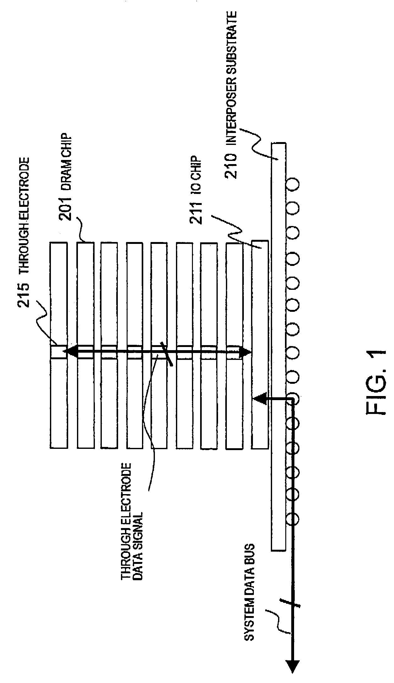
[0099]Referring to FIG. 1, a memory module according to the present invention is shown. The memory module shown in FIG. 1 is capable of inputting / outputting a data signal corresponding to a data width of a plurality of DRAM chips as a memory data bus width in the same manner as in the memory module shown in FIG. 40. The memory module shown in FIG. 40 can be formed in a stacked structure shown in FIG. 1 in this manner to constitute a memory system including a plurality of memory sub-systems in the whole memory system and having a data rate of 12.8 GBps in each memory sub-system and capable of increasing a memory capacity by expansion and reducing a mounting area.

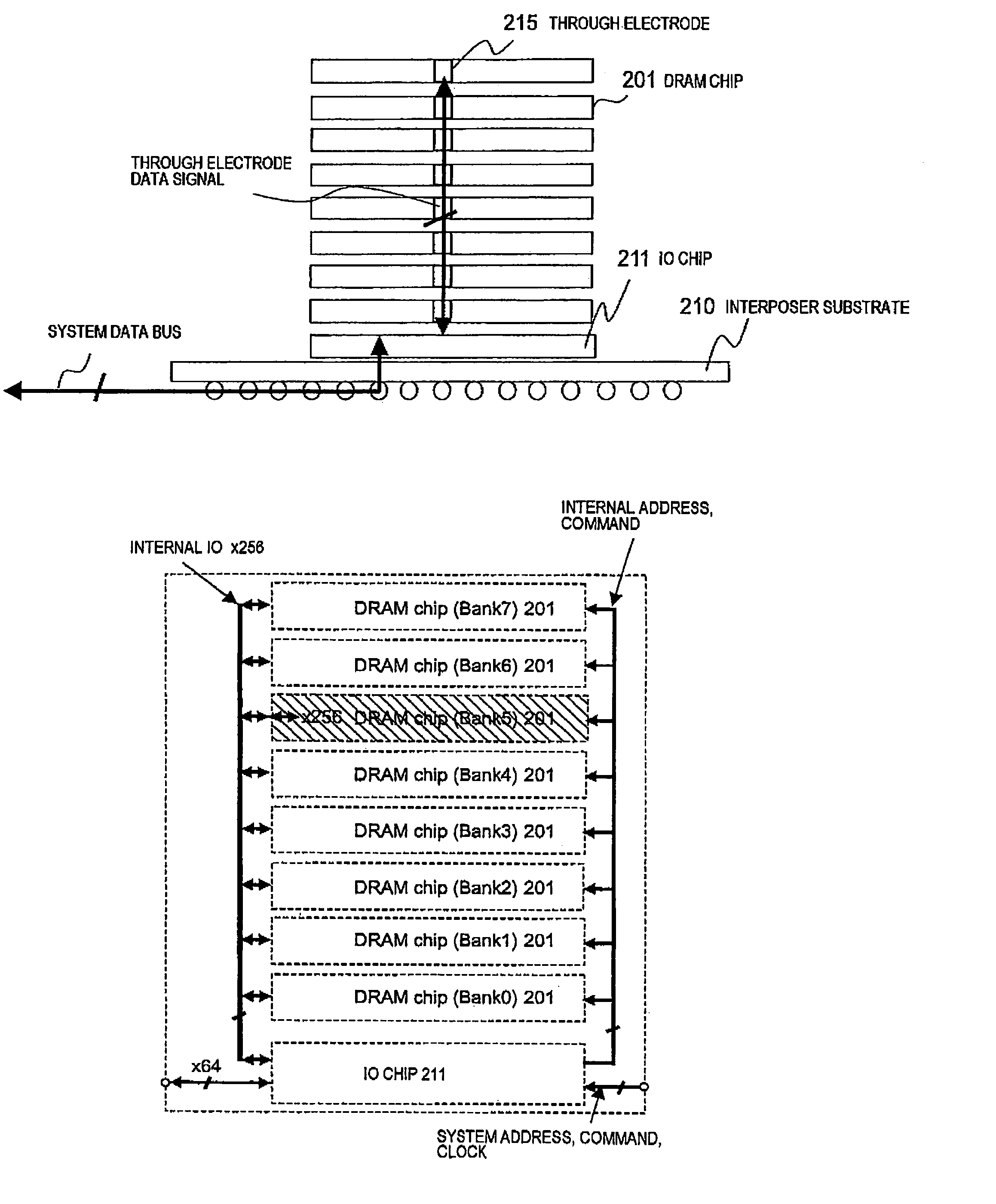
[0100]The shown memory module comprises an interposer substrate 210, an IO chip 211 mounted on the interposer substrate 210, and eight DRAM chips 201 stacked on the IO chip 211. Here, first to eighth DRAM chips will be referred to upwards from the DRAM chip of a lowermost layer adjacent to the IO chip 211. The memory module m...

second embodiment

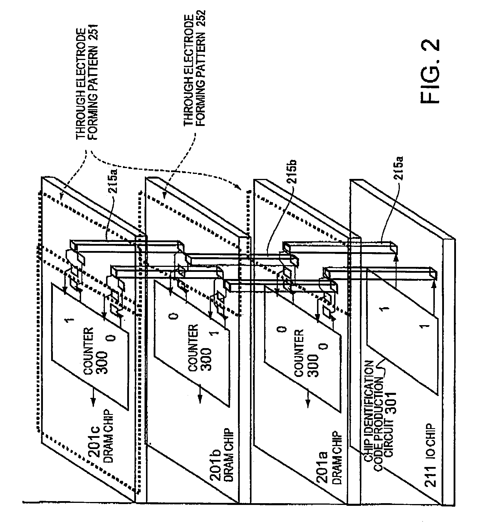
[0114]The memory module according to the present invention will be described with reference to FIG. 2. Each DRAM chip 201 shown in FIG. 2 comprises a counter circuit 300 which produces a collation signal with which a control signal or an address signal transmitted from the IO chip 211 is collated to receive a signal, and a chip identification code production circuit 301 is disposed in the IO chip 211.

[0115]Furthermore, as shown in FIG. 2, DRAM chips 201a and 201c comprises the same through electrode forming pattern 251. On the other hand, a DRAM chip 201b comprise a through electrode forming pattern 252 different from the through electrode forming pattern 251 of the DRAM chips 201a and 201c. The IO chip 211 is connected to the through electrode forming pattern 251 of the DRAM chip 201a by through electrodes 215a, the DRAM chip 201a is connected to 201b by through electrodes 215b, and further the DRAM chip 201b is connected to 201c by the through electrodes 215a. Only two through ele...

third embodiment

[0160]Referring to FIG. 16, the memory module according to the present invention is shown. The memory module can have a memory capacity equal to that of a conventional 2-rank memory module. For the shown memory module, a constitution suitable for a case where two DRAM chips 201 are simultaneously objects of access is shown.

[0161]Specifically, for the memory module, two IO chips 211a and 211b mounted on the interposer substrate (not shown), and four layers of DRAM chips 201a, 201b on the IO chips 211a, 211b are stacked, and the DRAM chips 201a, 201b on the respective IO chips 211a and 211b are simultaneously accessed one by one to constitute a 2-rank memory module. In this case, the data signals of ×256 bits are transmitted / received between the simultaneously accessed DRAM chips 201a, 201b and IO chips 211a and 211b, and the system data signals of ×32 bits are transmitted / received between the respective IO chips 211a and 211b and the chip set. In the drawing, a pair of DRAM chips 201...


PUM


Abstract

In a memory module including a plurality of DRAM chips which transmit/receive a system data signal with a predetermined data width and at a transfer rate and which transmit/receive an internal data signal having a larger data width and a lower transfer rate as compared with the system data signal, it has become clear that there is a restriction on the transfer rate of the system data signal and that speeding-up cannot be expected. A current consumption in a plurality of DRAMs constituting the memory module is large, and this is also a factor for hindering the speeding-up. There is obtained a memory module in which a plurality of DRAM chips are stacked on an IO chip and in which each DRAM chip is connected to the IO chip by a through electrode and which comprises a constitution for mutually converting the system data signal and the internal data signal in each DRAM chip by the IO chip. In this constitution, a wiring between the DRAM chips can be shortened, and DLL having a large current consumption may be disposed only on the IO chip.

Description

BACKGROUND OF THE INVENTION[0001](1) Field of the Invention[0002]The present invention relates to a memory system including a plurality of memory modules such as memory sub-systems, particularly to a memory system comprising a plurality of memory units in the respective memory modules.[0003](2) Description of the Related Art[0004]As this type of memory system, there has heretofore been a DRAM memory system comprising a constitution in which a plurality of memory modules are attached onto a mother board and these memory modules are controlled by a chip set (memory controller) and a plurality of DRAMs are mounted as memory units on the respective memory modules.[0005]For the above-described DRAM memory system, a system has been proposed in which a stub series terminated transceiver logic (SSTL) is used as interface standards and data can be written / read at a high rate and with a low signal amplitude using a double data rate (DDR) method for inputting / outputting data in synchronization...

Claims


Application Information

Patent Timeline
IPC IPC(8): G11C5/06G06F12/00G06F13/16G11C5/00G11C5/02G11C7/00G11C7/10H01L25/00H01L25/065H01L25/07H01L25/18
CPCG11C5/00H01L23/5384G11C5/06G11C7/1051G11C7/1063G11C29/1201G11C29/26G11C29/48H01L25/0657H01L25/18G11C8/12G11C11/408G11C5/04H01L2225/06513H01L2225/06517H01L2225/06541H01L2224/16H01L2924/00014H01L2224/16145H01L2224/0401F24C15/2035
Inventor MATSUI, YOSHINORISUGANO, TOSHIOIKEDA, HIROAKI
Owner LONGITUDE LICENSING LTD
Why Eureka
Try Eureka