Non-volatile memory device

a non-volatile, memory device technology, applied in the direction of digital storage, electric analogue stores, instruments, etc., can solve the problems of low reliability and high integration, low bias-voltage dependence of mr ratio of magneto resistive elements, and reduction of write magnetization variations. , to achieve the effect of improving the reliability of mram recording, reducing the bias-voltage dependence of mr ratio of magneto resistive elements, and high reliability

Inactive Publication Date: 2006-10-17
INT BUSINESS MASCH CORP
View PDF14 Cites 30 Cited by
  • Summary
  • Abstract
  • Description
  • Claims
  • Application Information

AI Technical Summary

Benefits of technology

[0018]It is an object of the invention to improve the reliability of MRAM recording. It is also another object of the invention to allow highly reliable reading of information, provided that a certain degree of variations in resistance values exists. It is a further object of the invention to lower the bias-voltage dependence of MR ratio of magneto resistive elements.
[0019]A brief summary of the present invention is given as follows. According to the invention, recording one bit of information in a memory cell includes a plurality of sub-cells each having magneto resistive elements connected in series or in parallel, and the memory cell is constructed such that a plurality of the magneto resistive elements are connected in series and in parallel in the whole memory cell by connecting the sub-cells in parallel or in series. This structure of the memory cell can reduce a current flowing through one magneto resistive element and thus suppress the deterioration in the reliability of the memory cell, caused by making the cell smaller. Because a plurality of the magneto resistive elements together record one bit of information, even if one of the magneto resistive elements have a smaller change in the resistance value, the reduced change in the resistance value of the whole memory cell can be made smaller. Further, when the magneto resistive elements are connected in series, the voltage applied to one element becomes small. Thereby, the bias-voltage dependence of the magneto resistive element becomes small, because, in the bias-voltage dependence of the magneto resistive element, the larger the voltage across one magneto resistive element is, the smaller the change in the resistance value (MR ratio) is.
[0020]Further, according to an aspect of the invention, a plurality of the memory cells connected in series or in parallel together may record one bit of information. The serial or parallel connection is made in a peripheral circuit of the memory cell. Thereby, in addition to the improvement of the reliability of recording information, the number of the memory cells used for recording one bit can be modified by changing the connections of interconnect lines in the peripheral circuit without changing the device design within the memory cell. For example, when the reliability of the magneto resistive elements is relatively low, the number of the memory cells used for recording one bit will be increased (that is, more memory cells are connected in series and in parallel), and when the reliability has been improved, one memory cell is used to record one bit.

Problems solved by technology

As described above, an MRAM device has noticeable advantages over other memory devices, but also it has various problems in achieving high reliability and high integration into comercial application.
For example, the problems include the reduction of variations in write magnetization and the stabilization of the pin layer.
In particular, because such an MRAM device uses tunnel current, the insulating layers need to be made extremely thin, and as such improving the stability and uniformity of the insulating layers are significant challenges.
For example, as MRAM cell size is reduced, the flow of current per unit area of the TMR cells becomes larger, resulting in a deterioration of the reliability.
This is one of factors for low reliability of the insulating layer in an extremely thin film.
There is another problem that the element resistances varies due to the manufacturing process variations in the insulating layers, pin layers, and free layers.
This may prevent appropriate reading of information.
That is, when variations in changed portions of the resistance values are large, it is difficult to detect a change in the resistance value dependent on the magnetization direction.
In addition, for a characteristic of magneto resistive elements, a problem has been pointed out that a change in the resistance value dependent on the magnetization direction (MR ratio) is reduced when a high bias voltage is applied to the magneto resistive elements.

Method used


Image

  • Non-volatile memory device
  • Non-volatile memory device
  • Non-volatile memory device

Examples


embodiment 1

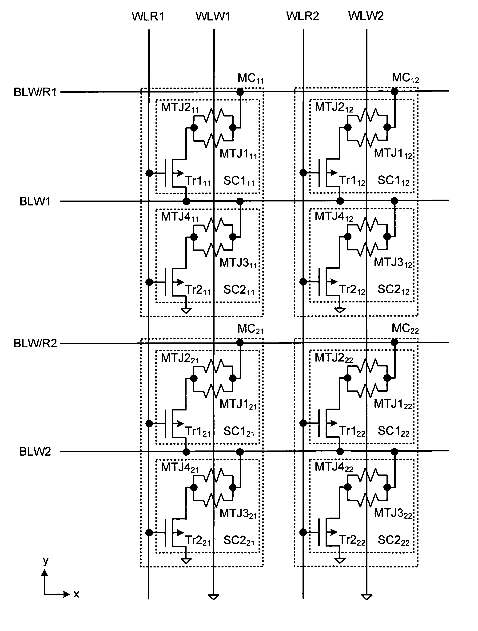
[0058]FIG. 3 shows a circuit diagram illustrating a potion of the memory cell area included in an example of a memory device according to another embodiment of the invention. As shown in FIG. 3, the memory device according to the present embodiment has read word lines WLR-1, WLR-2, write word lines WLW-1, WLW-2, and bit line BL. The word line (read word lines WLR-1, WLR-2, and write word lines WLW-1, WLW-2) is formed extending in a first direction (indicated as y direction in the figure). The bit line BL is formed extending in a second direction (indicated as x direction in the figure) nearly perpendicular to the first direction. The memory cells MC are disposed at the intersections of the word lines and the bit line BL. By the way, the numbers given to the bit lines and word lines and the subscripts given to the memory cells and others are in accordance with the same rule as in the

[0059]The memory cell MC includes sub-cells SC1 and SC2. The sub-cell SC1 includes magneto resistive e...

embodiment 2

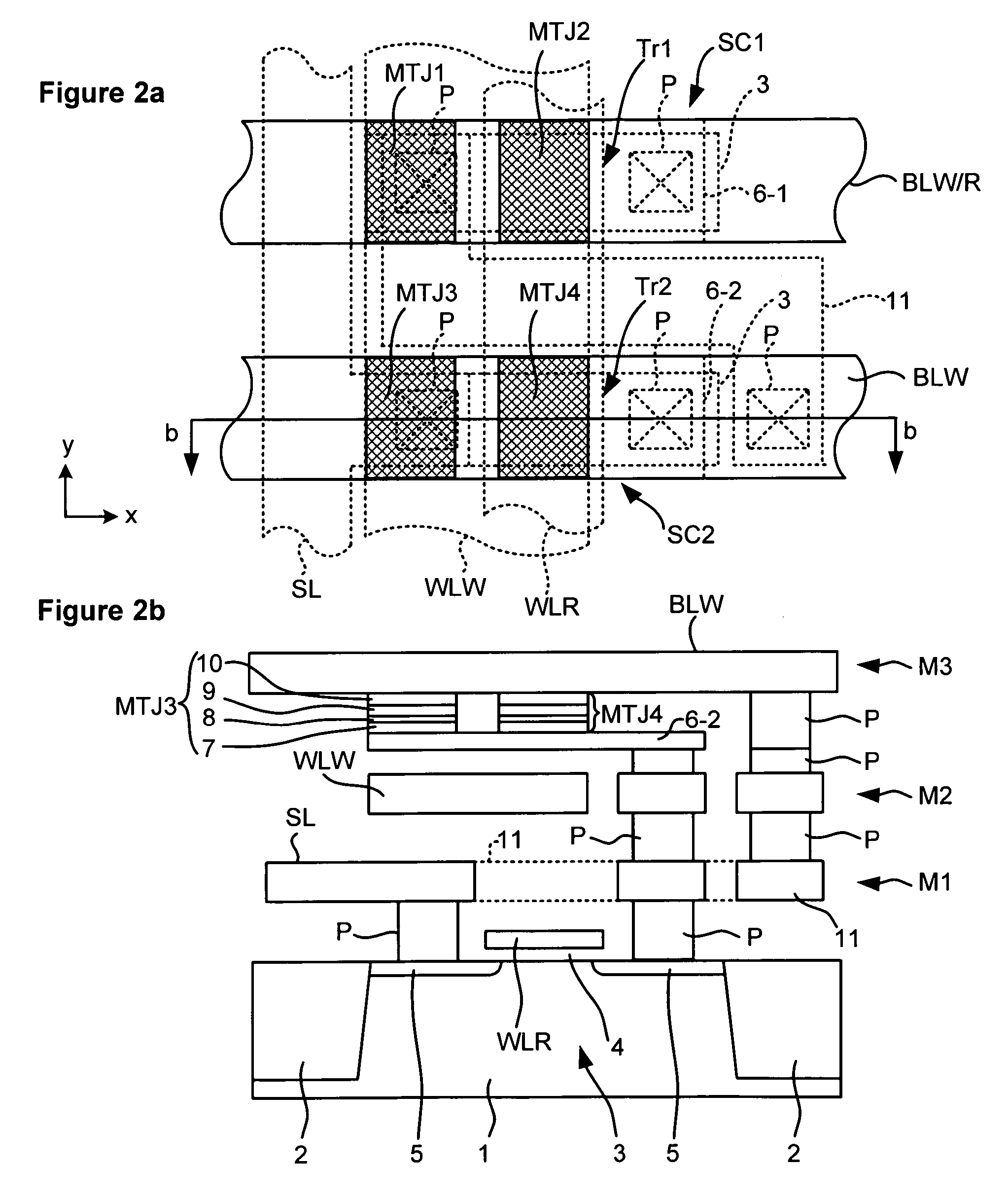
[0079]FIG. 7 is a plan view illustrating an example of a memory cell according to the present embodiment. MTJ1 and MTJ2 on one hand and MTJ3 and MTJ4 on the other hand are connected in parallel through the local interconnect lines disposed respectively at the tops and bottoms of the elements. Further, similar to the embodiment 2, the serial connection is implemented with local interconnect lines 13, 14 and a plug 15.

[0080]Such a device structure can implement the memory cell MC comprising the circuit shown in FIG. 6. However, the device structure shown in FIG. 7 is strictly for an illustration, and therefore other structures can implement the circuit of FIG. 6. Furthermore, it is natural that the above-described memory cell can make up a memory array when a plurality of the same memory cells are respectively arranged in the x and y directions.

[0081]Next, a method for writing and reading one bit of information to and from the above-described memory cell will be described. When data i...


PUM


Abstract

MRAM has read word lines WLR and write word line WLW extending in the y direction, write / read bit line BLW / R and write bit line BLW extending in the x direction, and the memory cells MC disposed at the points of the intersection of these lines. The memory MC includes sub-cells SC1 and SC2. The sub-cell SC1 includes magneto resistive elements MTJ1 and MTJ2 and a selection transistor Tr1, and the sub-cell SC2 includes magneto resistive elements MTJ3 and MTJ4 and a selection transistor Tr2. The magneto resistive elements MTJ1 and MTJ2 are connected in parallel, and the magneto resistive elements MTJ3 and MTJ4 are also connected in parallel. Further, the sub-cells SC1 and SC2 are connected in series between the write / read bit line BLW / R and the ground.

Description

[0001]This application is a division of application Ser. No. 10 / 057,369, filed Jan. 24, 2002, now U.S. Pat. No. 6,826,076.BACKGROUND OF THE INVENTION[0002]1. Field of the Invention[0003]This invention relates to a non-volatile memory device, and more particularly, it relates to a technology useful for a memory device which utilizes the Magneto Resistive (MR) effect enabled by the tunneling effect.[0004]2. Background of the Invention[0005]In recent years, attention has been given to a Random Access Memory (RAM) using the Magneto Resistive Effect, wherein the resistance value of a magnetic substance varies depending on the magnetization direction of the substance by virtue of Magneto Resistive Effect. RAM using the Magnetic Resistive Effect is referred to as MRAM (Magneto-resistive RAM) For the Magneto Resistive Effect, the anisotropic Magneto Resistive Effect (AMR) and giant Magneto Resistive Effect (GMR) are known. It has also been known that higher field sensitivity can be realized...

Claims


Application Information

Patent Timeline
Patent Type & Authority Patents(United States)
IPC IPC(8): G11C5/06G11C11/15G11C11/14G11C11/16H01L21/8246H01L27/105H01L43/08
CPCG11C11/16
Inventor MIYATAKE, HISATADANODA, KOHKISUNAGA, TOSHIOUMEZAKI, HIROSHIASANO, HIDEOKITAMURA, KOJI
Owner INT BUSINESS MASCH CORP
Why Eureka
Try Eureka