Method for implementing electro-static discharge protection in silicon-on-insulator devices

a technology of electrostatic discharge and silicon-on-insulator, which is applied in the direction of semiconductor devices, semiconductor/solid-state device details, electrical equipment, etc., can solve the problems of large electrostatic potential to be discharged across a device, failure of electronic devices and components, and devices formed on soi wafers that are just as susceptible to esd events as bulk silicon devices, etc., to achieve better esd protection

Inactive Publication Date: 2006-10-24
ALTERA CORP
View PDF4 Cites 29 Cited by
  • Summary
  • Abstract
  • Description
  • Claims
  • Application Information

AI Technical Summary

Benefits of technology

[0011]The present invention addresses the aforementioned problems by utilizing the parasitic bipolar characteristics of NMOS and PMOS devices. A shared source-drain region between two stacked gate NMOS or PMOS devices is formed such that the depth of the dopant in the shared region does not extend through the silicon layer to the insulating layer. This allows the two NMOS or PMOS devices to share a common body, and thus a single parasitic bipolar transistor is formed between the drain of one NMOS or PMOS device and the source of the second NMOS or PMOS device. Two or more NMOS or PMOS devices in stacked gate configurations formed on SOI in accordance with embodiments of the present invention exhibit simultaneous snapback. As a result, snapback typically occurs at a lower voltage than for two or more such devices not operating in simultaneous snapback, thereby providing better ESD protection to the devices by allowing the bipolar effect to start earlier during an ESD event.
[0012]A further embodiment includes a method for forming two or more stacked gate NMOS or PMOS devices on SOI. Without altering the number of process steps, the method protects the shared source-drain region between two NMOS or PMOS devices during a final doping step and silicide processing. As such, the dopant in the shared region is limited in depth so that it does not extend through the silicon layer to the insulating layer.

Problems solved by technology

However, devices formed on SOI wafers are just as susceptible to ESD events as bulk silicon devices.
ESD events may take various forms, but essentially they cause a large electrostatic potential to be discharged across a device.
The energy associated with such ESD events often leads to failure of electronic devices and components.
The damage is typically thermal in nature and often leads to device or interconnect burnout.
Such high currents may lead to on-chip voltages that are high enough to cause oxide breakdown in thin gate MOS processes.
If the gate-channel breakdown voltage of a MOS device is exceeded during an ESD event, a hole will be burned through the oxide insulator of the gate and the transistor will be destroyed.
However, not every ESD event can be prevented.
The problem with such protection circuits is that they use substantial layout area and raise the cost of the device.
None of the aforementioned techniques consistently provide effective and efficient ESD protection in SOI, and a need remains for an improved means of ESD protection in stacked gate devices formed on SOI.
In addition, such protection would not expand the required layout area for the device, nor would it add to the cost of manufacturing the device.

Method used


Image

  • Method for implementing electro-static discharge protection in silicon-on-insulator devices
  • Method for implementing electro-static discharge protection in silicon-on-insulator devices
  • Method for implementing electro-static discharge protection in silicon-on-insulator devices

Examples


Embodiment Construction

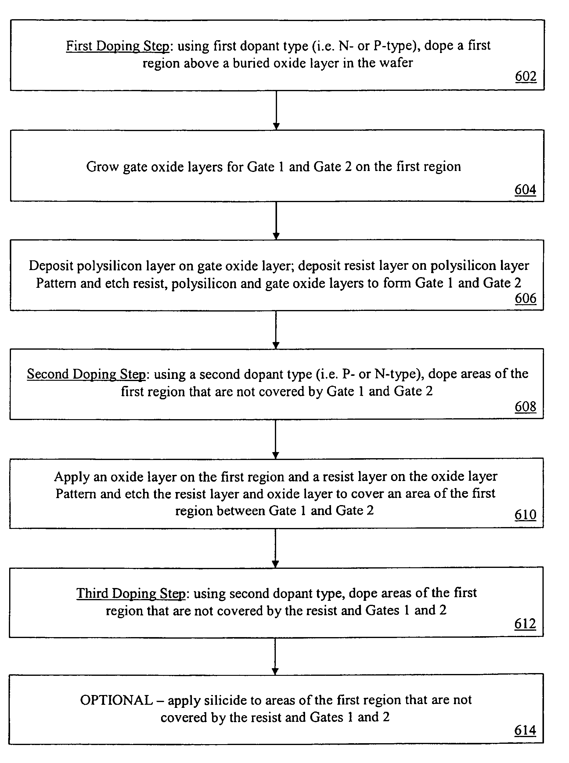
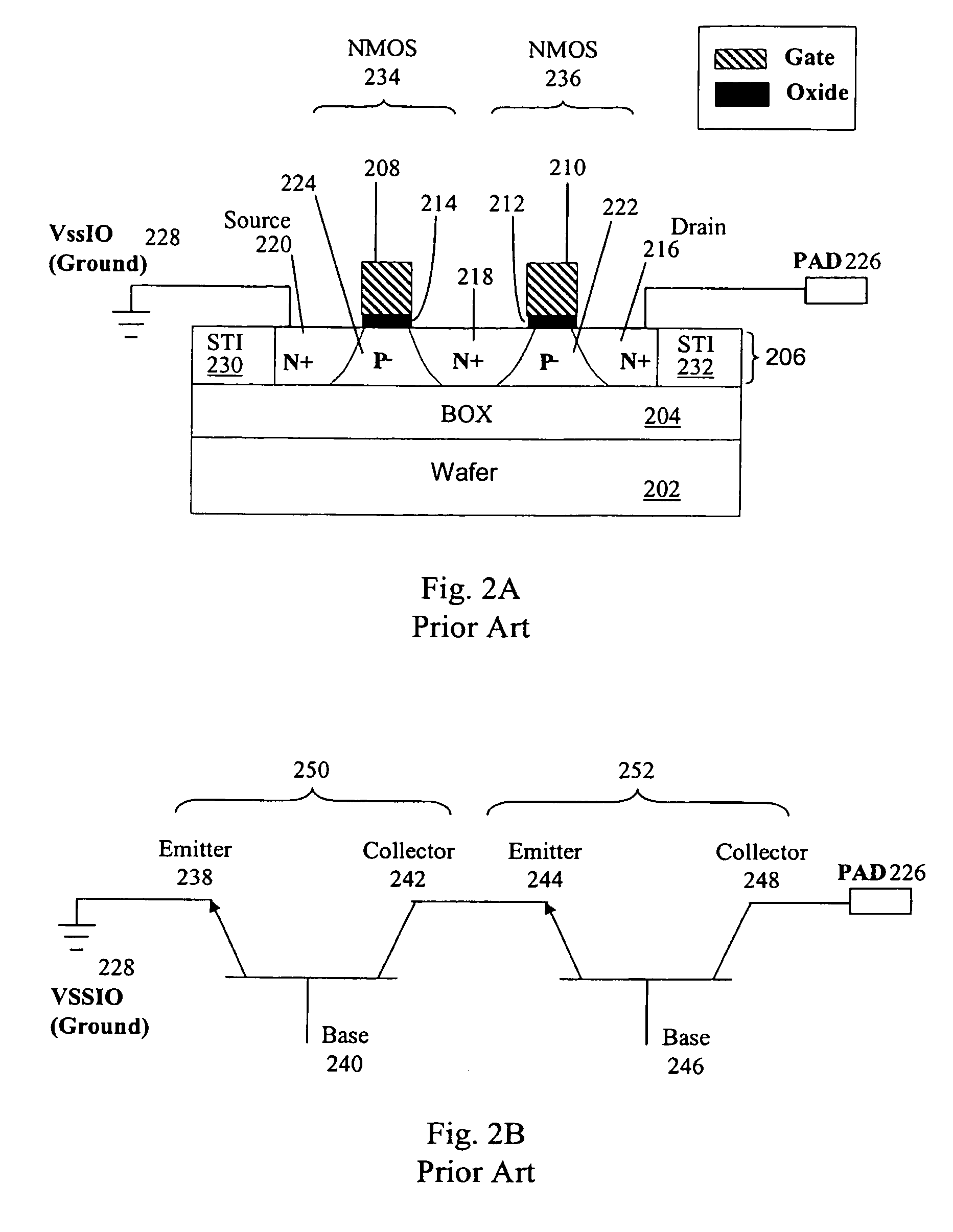
[0021]Embodiments of the present invention utilize the parasitic bipolar transistors in MOS devices to provide ESD protection to two or more such devices coupled together in series, such as in a stacked gate configuration. As illustrated in FIGS. 2A and 2B, typical prior art stacked gate devices formed on SOI have diffusion regions that extend down to the buried oxide layer, splitting the P− well region into two separate P− regions (222, 224). Thus, two such adjacent MOS devices do not share a common body. As illustrated in FIG. 2A, for example, first and second NMOS transistors 234, 236 in a stacked gate configuration are formed on a wafer 202 (e.g., a silicon wafer) with a buried oxide (BOX) layer 204. The NMOS transistors are formed in the silicon layer 206 above the BOX layer 204, and are isolated from other regions on the wafer by shallow trench isolation (STI) regions 230, 232. NMOS transistor 234 includes a N+ doped source region 220, a P− doped body region 224, an N+ doped d...


PUM


Abstract

The present invention is a method and apparatus whereby two NMOS or PMOS devices connected in series in a stacked gate configuration formed on SOI exhibit improved ESD response characteristics. The shared source-drain region between the two devices is formed to have a dopant depth in the shared region that does not extend through the silicon layer to the BOX layer. This provides a common body for the two devices, and thus a single parasitic bipolar transistor is formed between the drain of one NMOS or PMOS device and the source of the second NMOS or PMOS device. Simultaneous snapback occurs for the two devices through the common body. A further embodiment includes a method of forming two or more stacked gate NMOS or PMOS devices on SOI. The method includes protecting the shared source-drain region between two NMOS or PMOS devices during a final doping step and silicide processing.

Description

CROSS-REFERENCE TO RELATED APPLICATION[0001]This application is a divisional of application Ser. No. 10 / 687,420 filed Oct. 15, 2003 now U.S. Pat. No. 6,906,387 which is incorporated herein in its entirety.FIELD OF INVENTION[0002]The present invention relates generally to semiconductor devices, and particularly to electrostatic discharge (ESD) protection in stacked gate semiconductor devices manufactured using silicon-on-insulator (SOI) technology.BACKGROUND OF THE INVENTION[0003]This invention is especially useful for protecting semiconductor devices from ESD events, and especially for protecting stacked gate metal oxide semiconductor (MOS) devices formed on silicon-on-insulator (SOI) wafers. SOI technology involves the formation of transistors in a thin layer of semiconductor material (e.g., silicon) overlaying a layer of insulating material (e.g., silicon dioxide). Typically, SOI wafers have a sandwich structure with an insulating layer between two silicon layers, one on either si...

Claims


Application Information

Patent Timeline
Patent Type & Authority Patents(United States)
IPC IPC(8): H01L21/84H01L23/62H01L27/02
CPCH01L27/0266
Inventor REESE, DIRK ALANMCELHENY, PETERLIANG, MINCHANG
Owner ALTERA CORP
Why Eureka
Try Eureka