Circuit carrier

a technology of circuit carrier and contact pad, which is applied in the direction of resisting details, sustainable manufacturing/processing, and final product manufacturing, etc., can solve the problems of large deterioration of the connection strength between the bump and the contact pad, and the contact pad is large, so as to improve the connection strength

Active Publication Date: 2006-10-24
VIA TECH INC
View PDF4 Cites 13 Cited by
  • Summary
  • Abstract
  • Description
  • Claims
  • Application Information

AI Technical Summary

Benefits of technology

[0010]The present invention provides a circuit carrier, applied in the package structure, which enhance the connection strength between the bump of the chip and the contact pad of the carrier by providing more pre-solder paste.
[0012]As embodied and broadly described herein, due to the stepped opening of the solder mask layer for accommodating more pre-solder paste, the structure of the present invention affords better connection strength between the bump and the contact pad. Moreover, an electro-migration resistive layer can be further included between the contact pad and the pre-solder paste, for increasing the electro-migration resistance. Hence, less inter-metallic compounds are generated in the interface and the connection strength can be maintained over a longer period, thus increasing the reliability and quality of the package structure.

Problems solved by technology

However, larger the opening becomes, larger the contact pad becomes.
Because these inter-metallic compounds are fragile, the connection strength between the bumps and the contact pads is greatly deteriorated, which often leads to disconnection.
Furthermore, electro-migration can even result in shorts.

Method used


Image

  • Circuit carrier
  • Circuit carrier
  • Circuit carrier

Examples


Embodiment Construction

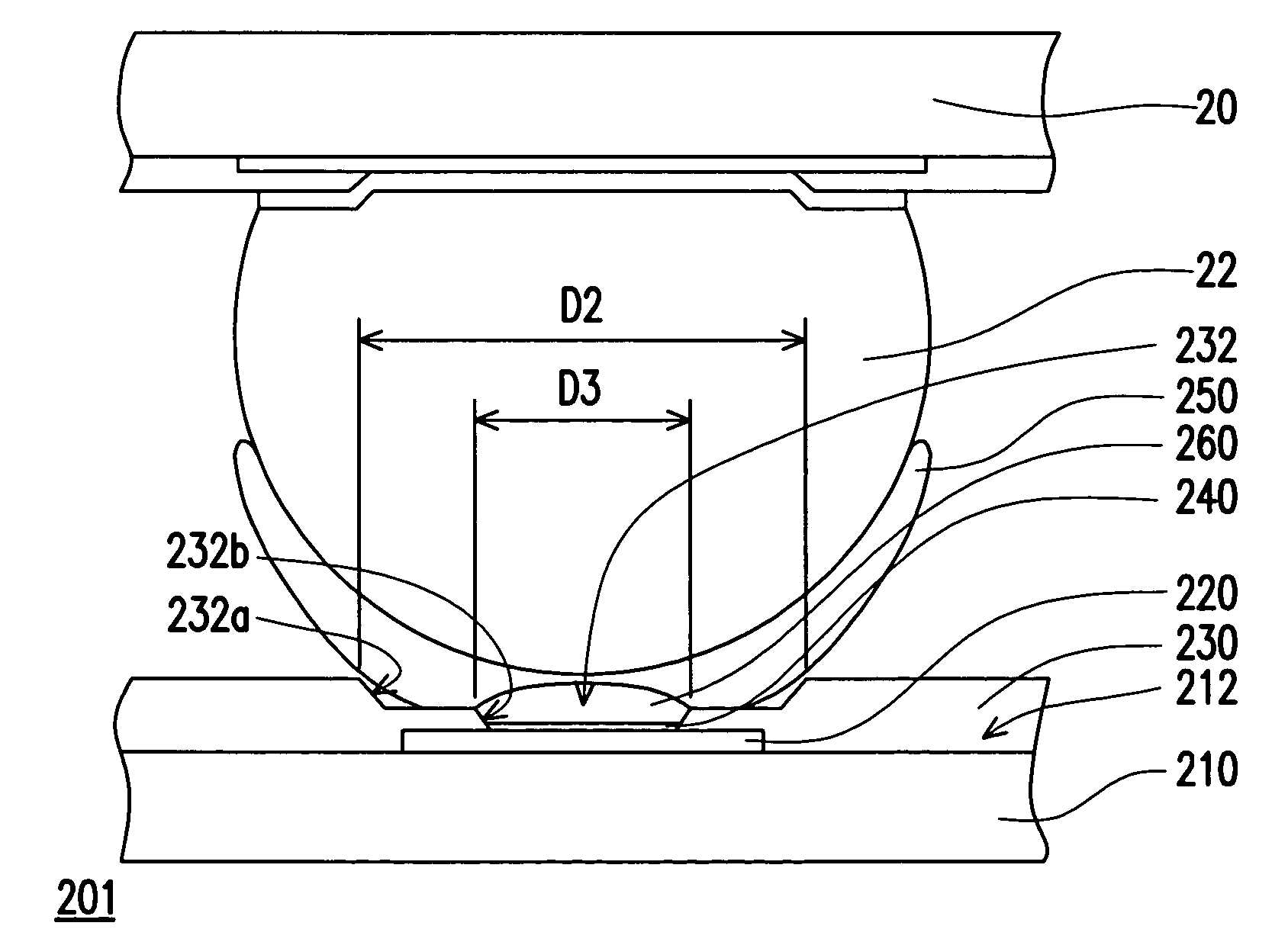
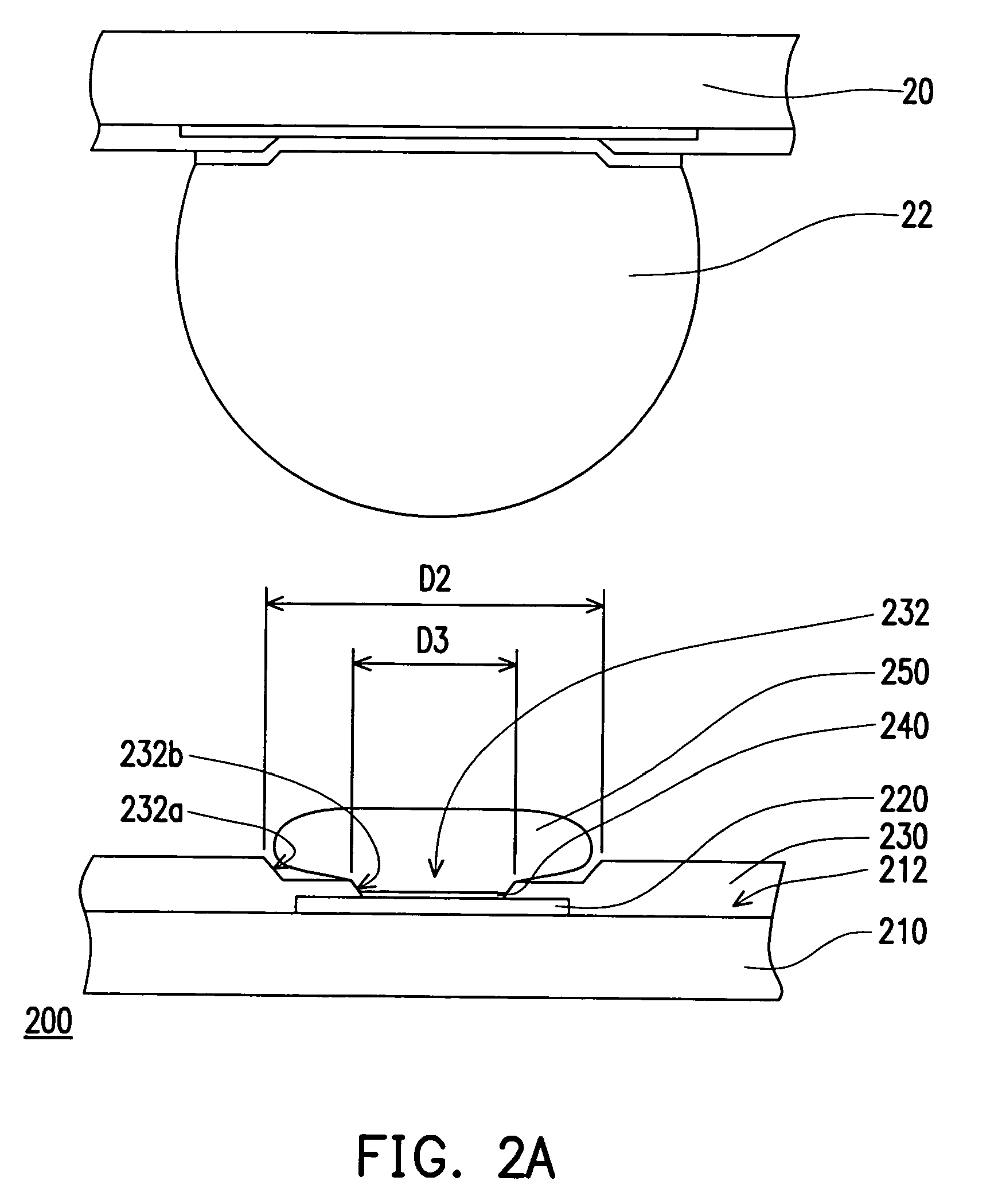
[0018]FIG. 2A is a schematic cross-sectional view illustrating a circuit carrier before connecting the pre-solder paste and the bump. The circuit carrier 200 includes at least a substrate 210, a plurality of contact pads 220 (only one is shown), a solder mask layer 230, a passivation layer 240 and a pre-solder paste 250. The substrate 200, for example, a laminated substrate, includes a plurality of conductive layers, a plurality of insulation layers disposed alternatively between two adjacent conductive layers and a plurality of through-holes, whereas each through-hole at least penetrates one insulation layer for connecting two conductive layers. The contact pads 220, disposed on a surface 212 of the substrate 210, are connected to a plurality of bumps 22 on the chip 20. The bumps 22 are solder bumps for flip chip connection, for example. The topmost (outermost) conductive layer of the substrate 210 may constitute the contact pads 220. In that case, since the conductive layer of the...


PUM


Abstract

The present invention provides a circuit carrier for connecting to at least a bump. The circuit carrier comprises a substrate, at least a contact pad on a surface of the substrate and a solder mask layer covering the substrate. The solder mask has at least a stepped opening that exposes a portion of the contact pad. The stepped opening includes at least a first opening and a second opening and the size of the first opening is larger than that of the second opening. The stepped opening of the solder mask layer can contain more pre-solder paste, thus increasing the bonding strength between the bump and the contact pad.

Description

CROSS-REFERENCE TO RELATED APPLICATION[0001]This application claims the priority benefit of Taiwan application serial no. 93104722, filed on Feb. 25, 2004.BACKGROUND OF THE INVENTION[0002]1. Field of Invention[0003]The present invention relates to a circuit carrier. More particularly, the present invention relates to a circuit carrier having a solder mask layer with a stepped opening.[0004]2. Description of Related Art[0005]The flip chip interconnect technology for connecting bare dies (chips) to the carrier substrate can be summarized as follows. A plurality of pads are arranged on the active surface of the chip (die) in arrays and bumps are formed on the pads with the under bump metallurgy layer therebetween. The chip is facedown bonded (flipped) to be contact with the carrier substrate or the printed circuit board (PCB) via solder bumps. Since the flip chip technology has the advantages of achieving the high density of minimizing the package region and shortening the signal trans...

Claims


Application Information

Patent Timeline
Patent Type & Authority Patents(United States)
IPC IPC(8): H01L21/44H01L23/48H01L21/60H01L23/498H05K3/34
CPCH01L23/49816H01L24/81H05K3/3436H05K3/3452H01L2924/0002H01L2224/05572H01L2924/014H01L2224/81801H01L2924/01029H01L2924/01079H01L2924/01082H01L2924/19043H05K3/3484H05K2201/09845H05K2201/099H05K2201/10992H05K2203/0594H01L2924/01005H01L2924/01033H01L2924/0105H01L2924/00014H01L2224/05552H01L2224/0401H05K3/3485Y02P70/50
Inventor YANG, CHIH-AN
Owner VIA TECH INC
Why Eureka
Try Eureka