I-shaped and L-shaped contact structures and their fabrication methods

a contact structure and l-shaped technology, applied in the direction of semiconductor devices, electrical devices, transistors, etc., can solve the problems of limited reprogrammability, reduced storage densities, and limited memory classes, so as to reduce the size of semiconductor devices, improve design rules, and widen the process window

Active Publication Date: 2006-11-14
MACRONIX INT CO LTD
View PDF13 Cites 17 Cited by
  • Summary
  • Abstract
  • Description
  • Claims
  • Application Information

AI Technical Summary

Benefits of technology

[0012]The present invention has, for example, further application is semiconductor devices generally as it affords a means of fabricating ultra-small contacts thereby permitting further reduction in the sizes of semiconductor devices. Additionally, with fabrication methods of the present invention, each contact region is on only one side of the support structure (defined below), enabling better design rules and a wider process window, with no wasted structure. In illustrated embodiments, the memory material may comprise a phase-change material such as chalcogenide.
[0013]The method of the present invention employs deposition and etch processes known in the art of semiconductor processing which may be readily applied to produce relatively uniform results. The methods may also result in top electrodes that are self-aligned to the contact structures, forming self-aligned I-shaped or L-shaped contact structure arrays. This characteristic may additionally permit photo process windows to be enlarged. Additionally, the pitch of the support structure is twice that of the bit line, resulting in a pitch that is not very small, thus facilitating relative ease in control of the support structure etch process.

Problems solved by technology

A charge is stored on the gate of the field effect transistor to program each memory bit and has limited reprogrammability.
These classes of memories may also be relatively slow to program.
Although the memory cells of SRAMs, ROMs, EPROMs, EEPROMs, and flash memories do not require refreshing, they may suffer from disadvantages such as lower storage densities, larger size, and greater cost to manufacture compared to volatile DRAM devices.
One characteristic common among solid state memory devices including phase change memory devices is significant power consumption, particularly in setting or resetting memory elements.
Even as downscaling of component sizes continues, power consumption continues to be a significant consideration, particularly in portable devices that rely on power cells (e.g., batteries).
With conventional semiconductor processing technology, the minimum achievable dimensions of a contact for a chalcogenide memory device may be limited by photolithography tools.
Such dimensions may cause switching currents, voltages, and switching times to be too large and cycle life to be too small for integration with many leading-edge semiconductor technologies.
Additionally, conventional chalcogenide memory fabrication methods may not be able to efficiently and reliably produce the uniform memory elements needed for large-scale memory devices.

Method used


Image

  • I-shaped and L-shaped contact structures and their fabrication methods
  • I-shaped and L-shaped contact structures and their fabrication methods
  • I-shaped and L-shaped contact structures and their fabrication methods

Examples


Embodiment Construction

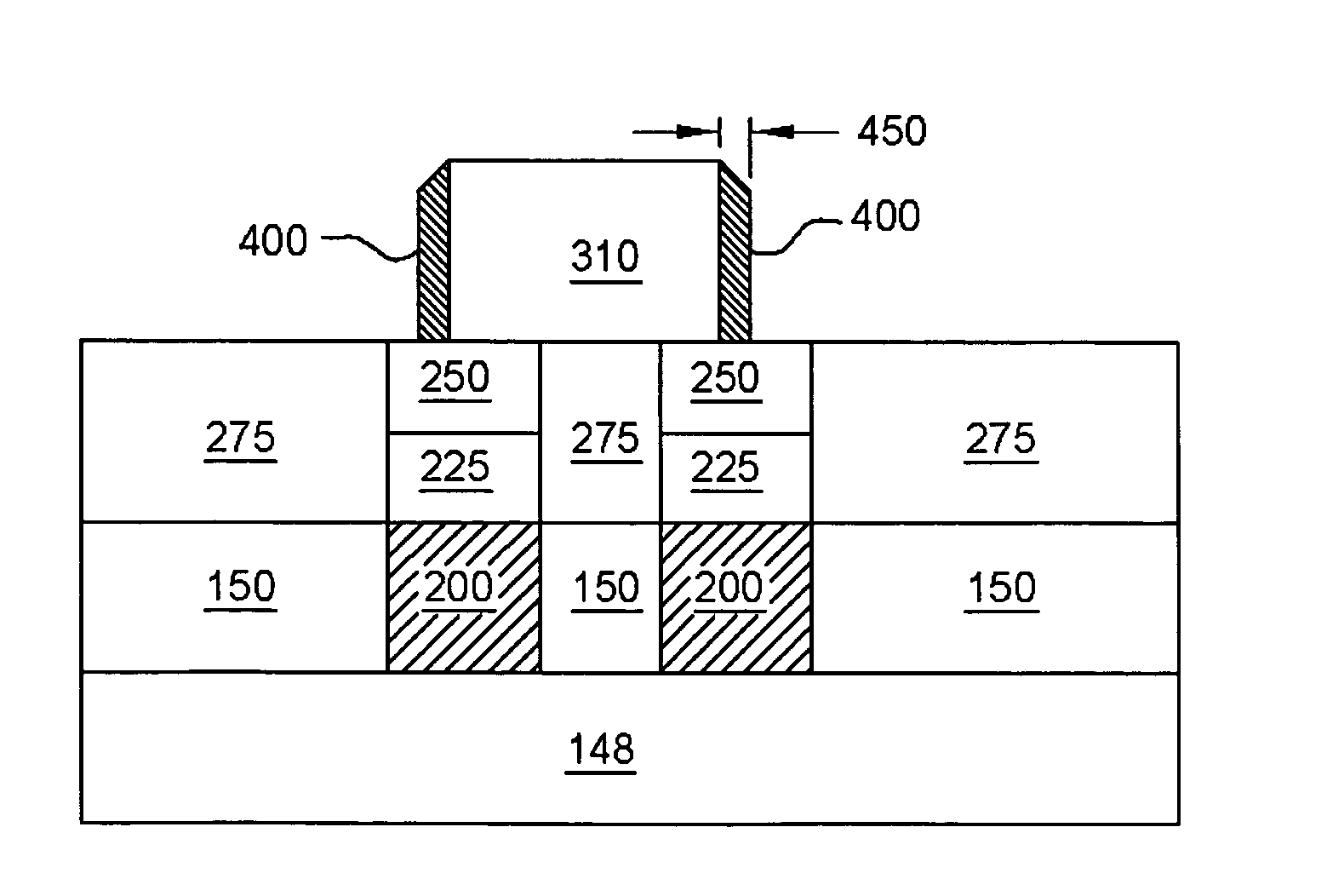
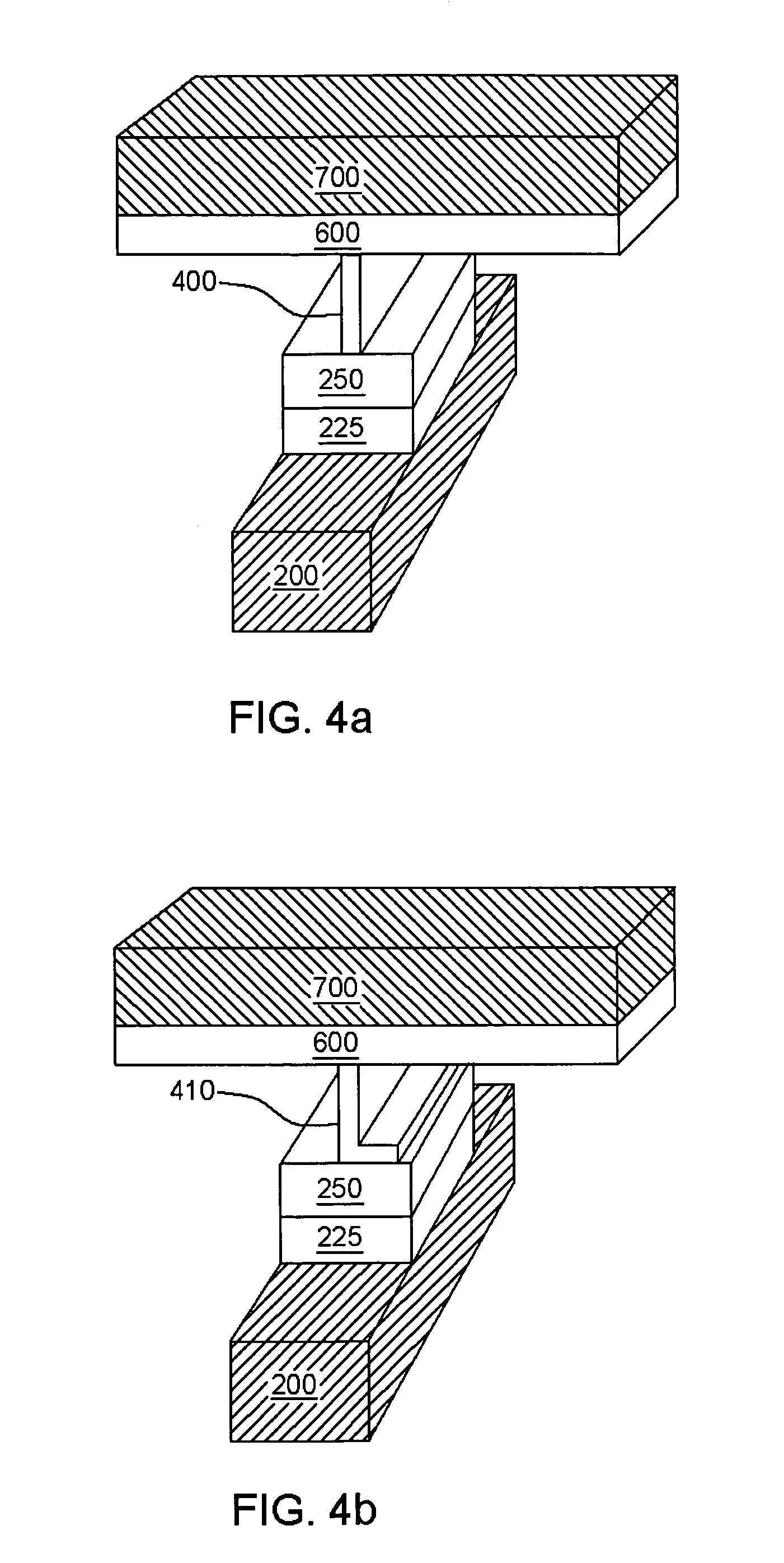
[0053]Reference will now be made in detail to the presently preferred embodiments of the invention, examples of which are illustrated in the accompanying drawings. Wherever possible, the same or similar reference numbers are used in the drawings and the description to refer to the same or like parts. It should be noted that the drawings are in simplified form and are not to precise scale. In reference to the disclosure herein, for purposes of convenience and clarity only, directional terms, such as, top, bottom, left, right, up, down, over, above, below, beneath, rear, and front, are used with respect to the accompanying drawings. Such directional terms should not be construed to limit the scope of the invention in any manner.

[0054]Although the disclosure refers to certain illustrated embodiments, it is to be understood that these embodiments are presented by way of example and not by way of limitation. The intent of the following detailed description, although discussing exemplary ...


PUM


Abstract

Contact structures having I shapes and L shapes, and methods of fabricating I-shaped and L-shaped contact structures, are employed in semiconductor devices and, in certain instances, phase-change nonvolatile memory devices. The I-shaped and L-shaped contact structures produced by these methods exhibit relatively small active areas. The methods that determine the contact structure dimensions employ conventional semiconductor deposit and etch processing steps that are capable of creating readily reproducible results.

Description

BACKGROUND OF THE INVENTION[0001]1. Field of the Invention[0002]This invention relates generally to semiconductor devices and fabrication methods and, more particularly, to methods for fabricating contacts for use in phase change memory devices.[0003]2. Description of Related Art[0004]Solid-state memory devices are used throughout the field of electronics. Typical memory applications include dynamic random access memory (DRAM), static random access memory (SRAM), read only memory (ROM), erasable programmable read only memory (EPROM), electrically erasable programmable read only memory (EEPROM), and flash memory. These can be divided into volatile and non-volatile memories. The primary element of the non-volatile devices, such as an EEPROM, typically employs a floating gate field effect transistor. A charge is stored on the gate of the field effect transistor to program each memory bit and has limited reprogrammability. These classes of memories may also be relatively slow to program...

Claims


Application Information

Patent Timeline
Patent Type & Authority Patents(United States)
IPC IPC(8): H01L27/108
CPCH01L21/76885H01L27/2409H01L27/2436H01L45/06H01L45/1233H01L45/1273H01L45/144H01L45/16H10B63/20H10B63/30H10N70/231H10N70/8418H10N70/826H10N70/8828H10N70/011
Inventor LEE, MING HSIULIU, RUICHEN
Owner MACRONIX INT CO LTD
Why Eureka
Try Eureka