Method of manufacturing device, device, and electronic apparatus

a manufacturing device and electronic equipment technology, applied in the direction of identification means, instruments, basic electric elements, etc., can solve the problems of increasing processing costs, poor utilization efficiency of raw materials, and difficulty in reducing manufacturing costs in the conventional manufacturing method

Inactive Publication Date: 2006-11-14
SEIKO EPSON CORP
View PDF13 Cites 21 Cited by
  • Summary
  • Abstract
  • Description
  • Claims
  • Application Information

AI Technical Summary

Benefits of technology

[0024]It is preferable that the insulating film for forming the partition wall is a polyimide film. By doing so, it is possible to form the partition wall easily. In particular, in case of using a photosensitive polyimide solvent, after the substrate has the polyimide solvent applied thereto and is dried, the region corresponding to an opening is exposed and developed to be remo

Problems solved by technology

However, in this conventional manufacturing method, there are disadvantages in that (1) since the process comprising the film formation and the etching is repeated many times, the manufacturing time is lengthened, (2) since most of the formed thin film is removed, the utilization efficiency of raw material is not good, and (3) since waste such as the etching s

Method used


Image

  • Method of manufacturing device, device, and electronic apparatus
  • Method of manufacturing device, device, and electronic apparatus
  • Method of manufacturing device, device, and electronic apparatus

Examples


Embodiment Construction

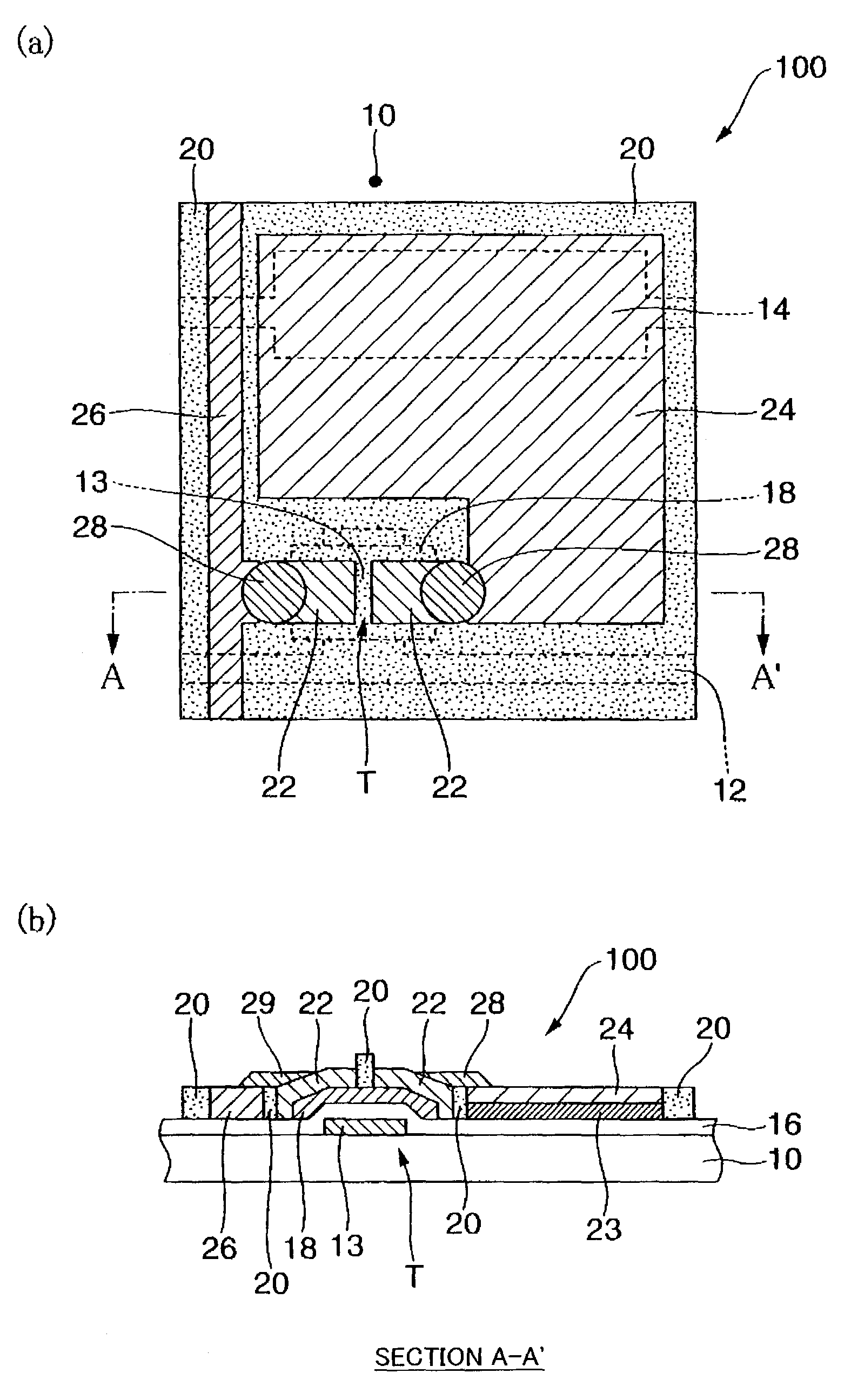
[0052]Now, a liquid crystal display device according to one embodiment of the present invention, and a method of manufacturing the same will be described with reference to the accompanying drawings.

[0053]In the present invention, the droplet ejection method is the method of forming a desired pattern, including an ejected material, by ejecting droplets to a desired region and may be referred to as the ink jet method. In this case, the droplet to be ejected is not so-called ink used for printing, but a liquid material containing materials constituting the device. For example, the materials include one capable of functioning as a conductive material or an insulating material which constitutes the device. Further, the droplet ejection is not limited to ejection by atomization, but includes continuous ejection of the liquid material drop by drop.

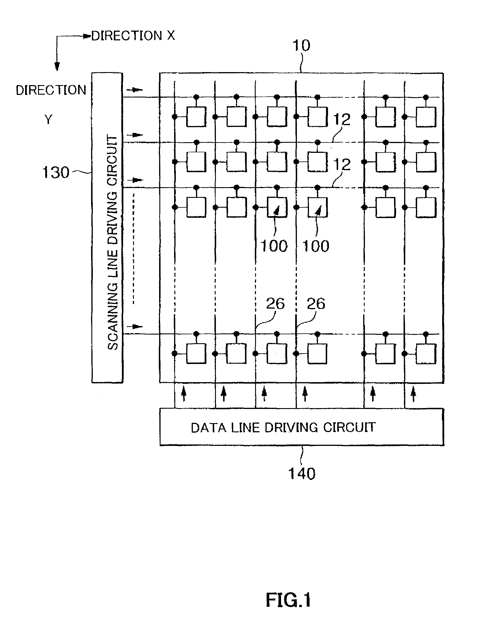
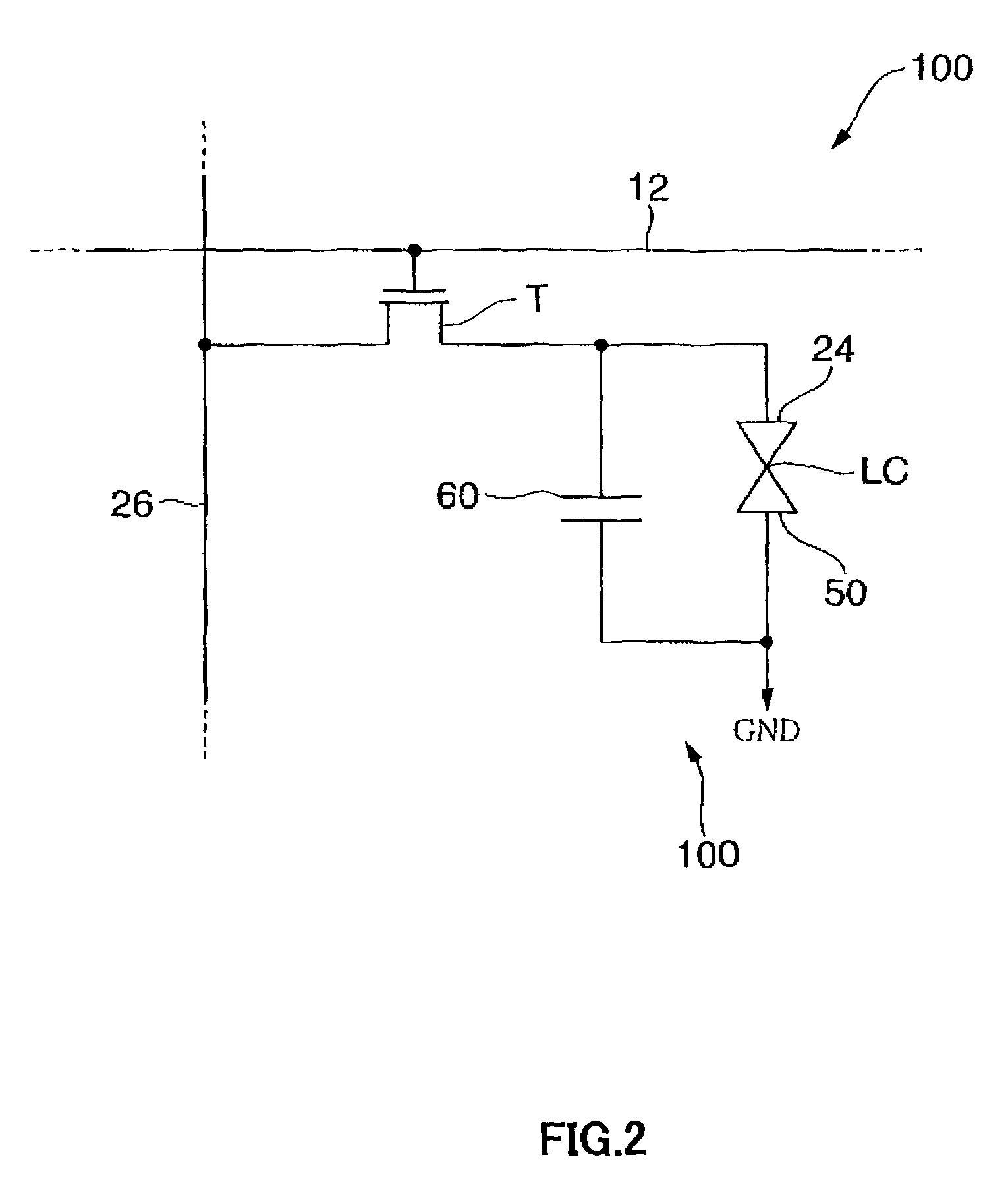
[0054]FIG. 1 schematically illustrates a configuration of a liquid crystal display device of this embodiment. The liquid crystal display device ...


PUM


Abstract

A pixel portion 100 of a liquid crystal display device comprises a thin film transistor T comprising a channel region 18, and source/drain regions 22, a source (data) line 26 for supplying current to the thin film transistor T, a color filter 23, and a pixel electrode 24. In forming the pixel portion 100, a gate electrode 13, a gate insulating film 16 and the channel region 18 are first formed on a glass substrate 10. On the glass substrate 10 after the formation of the channel region 18 is formed, a wall made of a polyimide film 20 surrounding the peripheries of the regions for forming the source/drain regions 22, the color filter 23, the pixel electrode 24 and the source line 26. Liquid materials are applied to the regions surrounded with a wall made of the polyimide film 20, and a heat treatment is carried out to form films, thereby forming elements such as the color filter 23 or the pixel electrode 24.

Description

BACKGROUND OF THE INVENTION[0001]1. Technical Field of the Invention[0002]The present invention relates to a method of manufacturing a device (for example, a liquid crystal display device or the like) comprising thin film elements such as thin film transistors, and a device manufactured by the method.[0003]2. Description of the Related Art[0004]Liquid crystal display devices have features of being thin and lightweight and have low power consumption, and thus they are used for various electronic apparatuses such as personal computers, mobile phones, digital still cameras, and liquid crystal televisions.[0005]The liquid crystal display device is provided with pixel portions using active elements such as thin film transistors. As the thin film transistor constituting the pixel portion, the inversely staggered type (or bottom gate type) structure constructed by forming a gate electrode on a substrate and laminating a semiconductor layer such as a channel region or a source / drain region,...

Claims


Application Information

Patent Timeline
IPC IPC(8): G02F1/1333G02F1/136G02F1/1335G02B5/20G02F1/1343G02F1/1362G02F1/1368G09F9/30H01L21/288H01L21/336H01L29/786
CPCG02F1/1362G02F1/133516G02F2001/136295G02F1/136295
Inventor FURUSAWA, MASAHIRO
Owner SEIKO EPSON CORP
Why Eureka
Try Eureka