
DAA hook switch

a technology of electronic hook switch and integrated circuit, which is applied in the direction of digital transmission, telephone line holding circuit, baseband system details, etc., can solve the problems of low control current available on the integrated circuit (ic) of the daa, and the need for at least one transistor, so as to achieve high impedance and high impedance

Inactive Publication Date: 2006-11-21
SILICON LAB INC
View PDF28 Cites 4 Cited by
  • Summary
  • Abstract
  • Description
  • Claims
  • Application Information

AI Technical Summary

Benefits of technology

[0013]The invention involves a telephone line interface circuit that is comprised of a first bipolar transistor having a base, emitter and collector, with the emitter being electrically coupled to the telephone line. A first resistor is coupled between the base and the emitter of the first transistor. A second bipolar transistor that includes a base, emitter and collector, is also included in the circuit and is connected in such a manner that the emitter of the second transistor is coupled to the base of the first transistor. A second resistor is coupled between the collector of the first transistor and the base of the second transistor. A line side circuit including a hook switch control is also part of the interface circuit.
[0014]The line side circuit has an off-hook power supply terminal that is coupled to the emitter of the second transistor, a hook switch control terminal that is coupled to

Problems solved by technology

However, electronic hook switches are constructed from high voltage transistors and have difficulties being, driven from integrated circuits fabricated in low voltage processes.
One difficulty is that the control current available on a DAA integrated circuit (IC) is very low.
Another difficulty is that often at least one transistor is required to high voltage level shift control outside of the operating voltage range of the controlling circuit.
In practice. the controlling IC is usually fabricated in a low cost 5 volt or less process and hence cannot be directly powered from the line voltage.
Although this method is quite effective, the power transformer is relatively expensive.
Although this method is low power, it is also relatively expensive, requiring an LED, a photovoltaic stack, and 1–2 high voltage MOS transistors in a specialized optical package.
This technique is less expensive than a transformer or optical solid-state switch but the high voltage isolation capacitors are moderately expensive.
Besides the hook switch function, the low voltage, line powered ICs in telephone or DAA circuits require external voltage regulations protection from high voltage transients, and loop current limiting for European use.

Method used


Image

  • DAA hook switch
  • DAA hook switch
  • DAA hook switch

Examples


Embodiment Construction

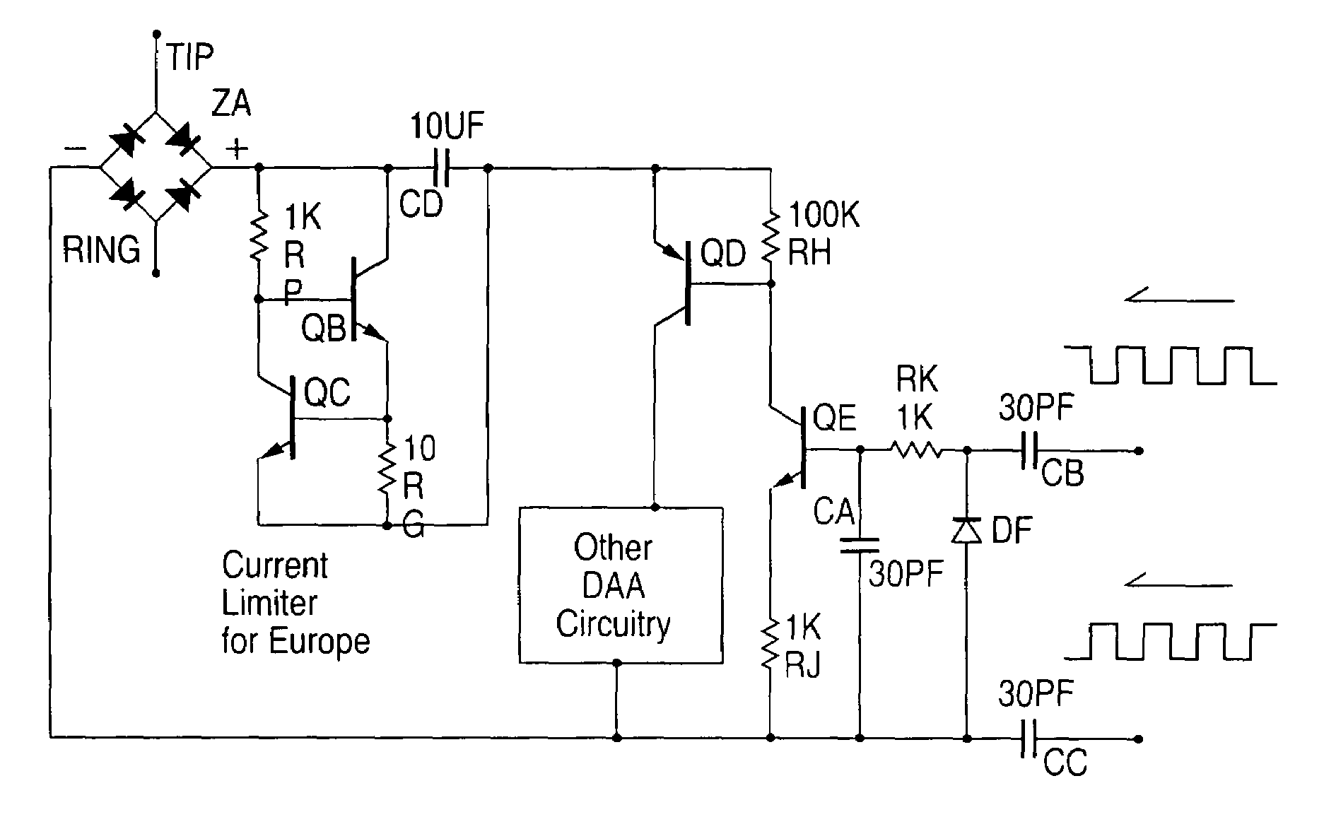
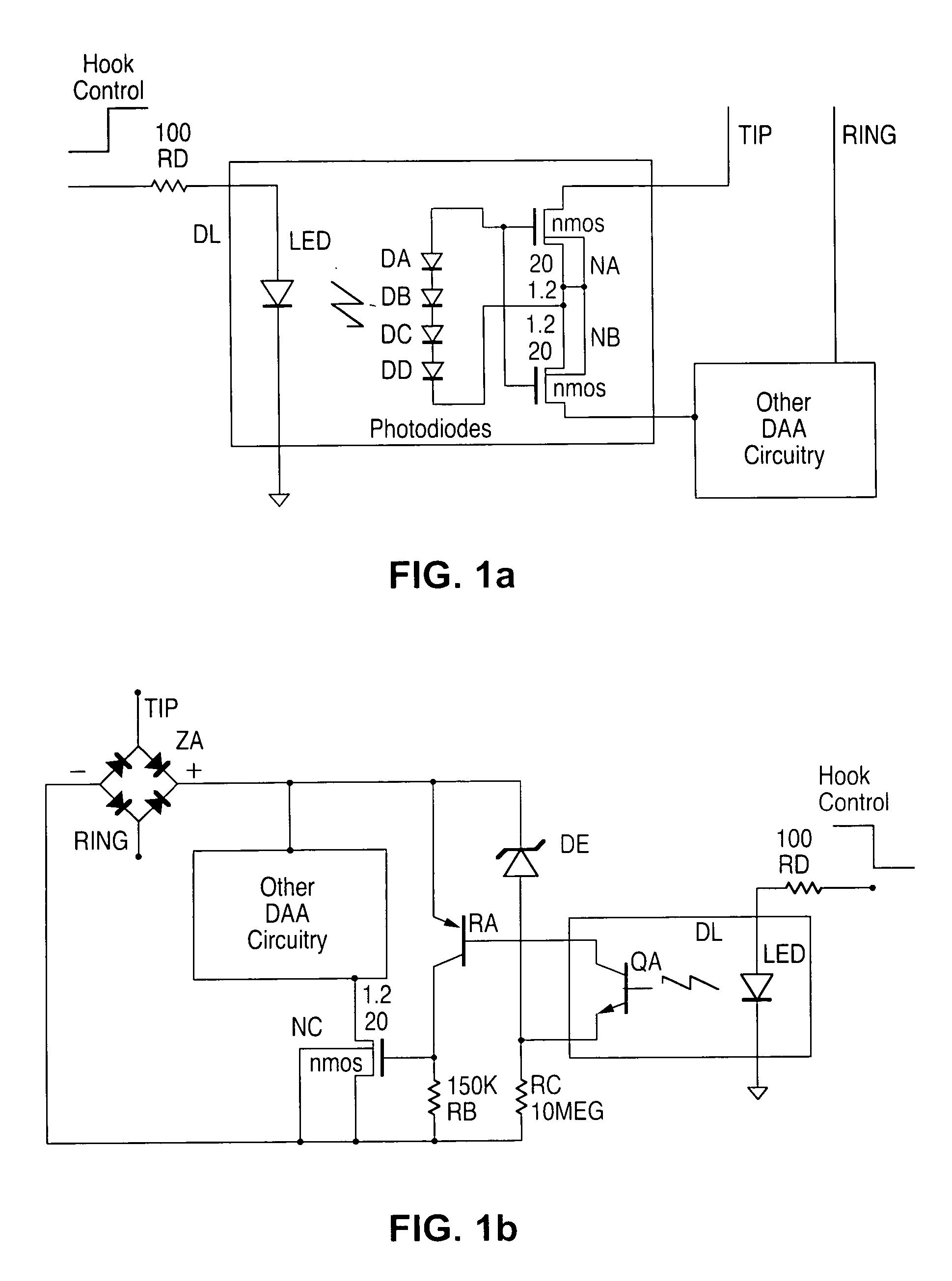
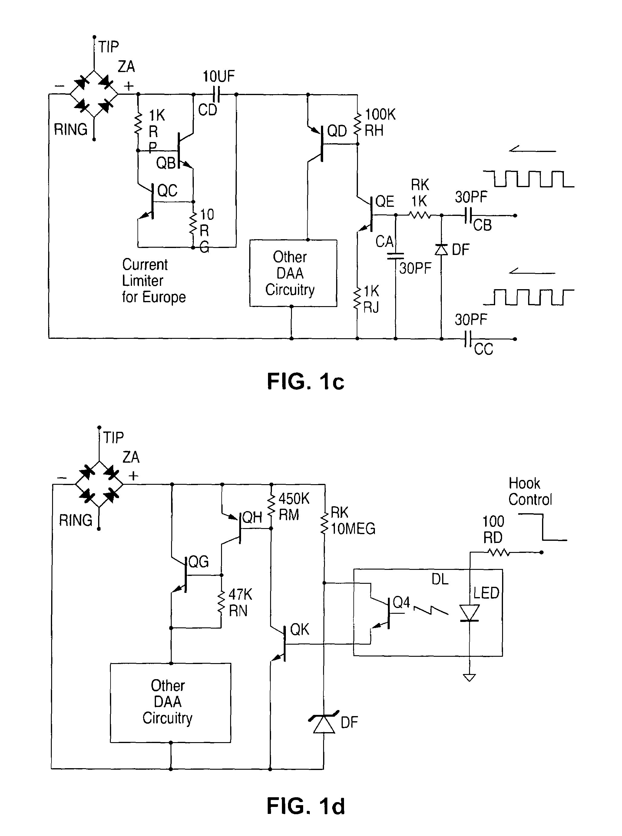
[0022]To achieve many of the functions needed or desired for electronic telephone or isolated DAA circuits, many extra and external components are typically utilized that add significant cost to the circuits. Therefore, in one aspect of the present invention, the complexity of the hook switch is reduced so that it can be fabricated with fewer and lower cost components while providing all of the functions discussed above.

[0023]In addition, for capacitor isolated DAA circuits, the capacitor driver receivers typically require additional input / output (I / O) pins. On large silicon ICs this is less of a problem. However, as advances in technology shrink IC die sizes down to the order of 1 square millimeter or smaller, ICs can become “I / O bound.” This means that the number of I / O pads defines the minimum size of the IC. Therefore, another aspect of the present invention is to permit the line side DAA IC design to be small and make it possible to multiplex I / O pins for multiple functions in ...


PUM


Abstract

A hook switch circuit is shown wherein two high-voltage bipolar transistors, a PNP transistor Q1 and a NPN transistor Q2. that are connected in a regenerative feedback manner to form a bi-stable latch. The regenerative structure permits the use of low beta transistors that may be turned on with a low control current, but still conduct a sufficient off-hook current. Also shown is a polarity steering regenerative switch (MP1, MP2) that provides a power supply voltage from a telephone line pair and may be adapted for a polarity signal and can be combined with a current mirror (MP7) to produce a current signal proportional to the line voltage (LV1).

Description

CROSS-REFERENCE TO RELATED PATENT APPLICATIONS[0001]This application claims priority from provisional patent application 60 / 446,971 filed Feb. 12, 2004, which is related to U.S. Pat. No. 5,946,393 and is a continuation-in-part of co-pending U.S. patent application Ser. No. 10 / 013,901 for a METHOD AND APPARATUS FOR ISOLATION IN A DATA ACCESS ARRANGEMENT USING ANALOG ENCODED PULSE SIGNALING filed Oct. 30, 2001, and Ser. No. 10 / 341,760 for a METHOD AND APPARATUS FOR PULSE WIDTH MODULATION SIGNAL RECOVERY USING HIGH SPEED CLOCK SIGNAL WITH PHASES filed Jan. 14, 2003, which claims the benefit of U.S. Provisional Patent Application No. 60 / 348,963, filed Jan. 14, 2002, herein incorporated by reference in their entirety for all purposes.FIELD OF THE INVENTION[0002]The present invention is directed toward improvements in an electronic hook switch for use in a telephone line interface or a Data Access Arrangement (DAA).BACKGROUND OF THE INVENTION[0003]For telephone interfaces or for isolated ...

Claims


Application Information

Patent Timeline
IPC IPC(8): H04M1/80H04B14/02H04L25/49H04M1/738
CPCH04B14/026H04L25/0268H04L25/4902H04M1/738
Inventor HOLCOMBE, WAYNE T.PARDOEN, MATTHIJS D.
Owner SILICON LAB INC
Learn More