Semiconductor device having solder bumps reliably reflow solderable

a technology of semiconductor devices and bumps, which is applied in the direction of sustainable manufacturing/processing, final product manufacturing, transportation and packaging, etc., can solve the problems of heat resistance properties of the substrate and other electric parts (such as electrolytic capacitors and etc.) mounted on the substrate, and achieve the effect of high reliability

Inactive Publication Date: 2006-12-05
RENESAS ELECTRONICS CORP
View PDF21 Cites 47 Cited by
  • Summary
  • Abstract
  • Description
  • Claims
  • Application Information

AI Technical Summary

Benefits of technology

[0010]The object of the invention is to realize solder bonding of high reliability in which th...

Problems solved by technology

Thus, by setting the reflow temperature so that these Pb-free solder bumps may be melted, the temperature of the substrate or the semiconductor device itself becomes higher by the value of 15 to 20° C. than the temperature measured between the ...

Method used


Image

  • Semiconductor device having solder bumps reliably reflow solderable
  • Semiconductor device having solder bumps reliably reflow solderable
  • Semiconductor device having solder bumps reliably reflow solderable

Examples


Embodiment Construction

[0030]The preferred embodiments of the invention are described below while referring to the drawings.

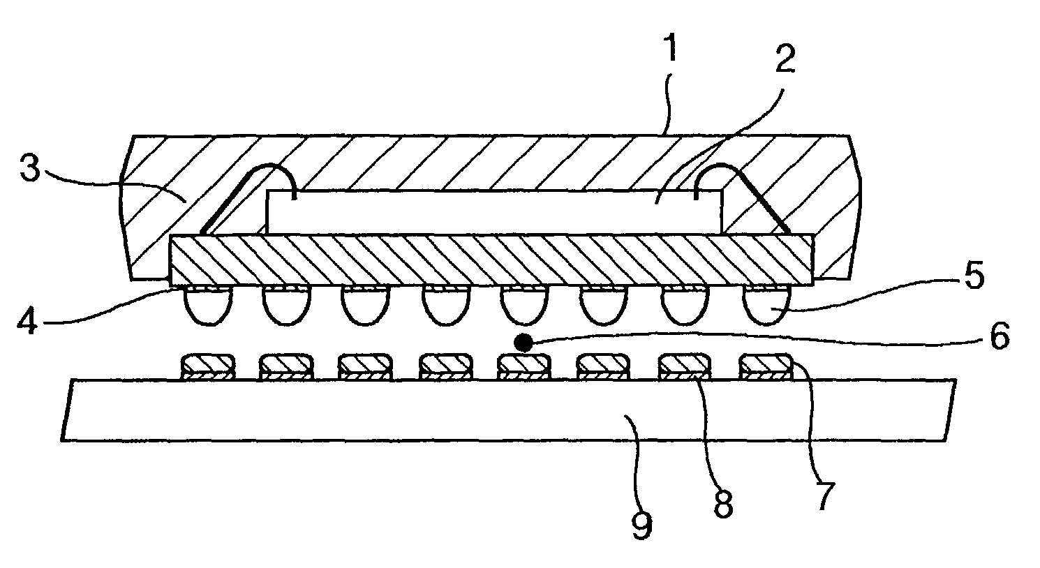
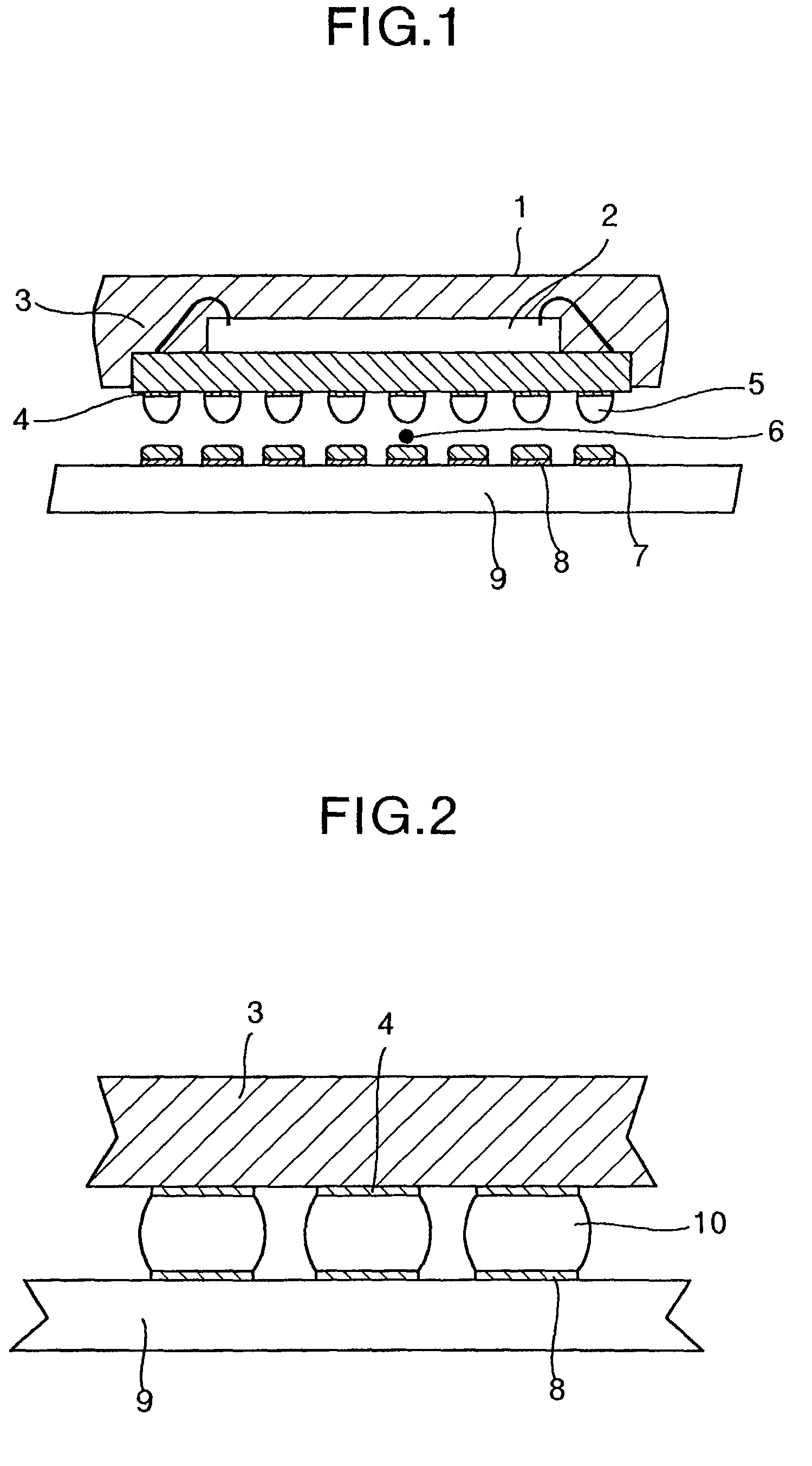
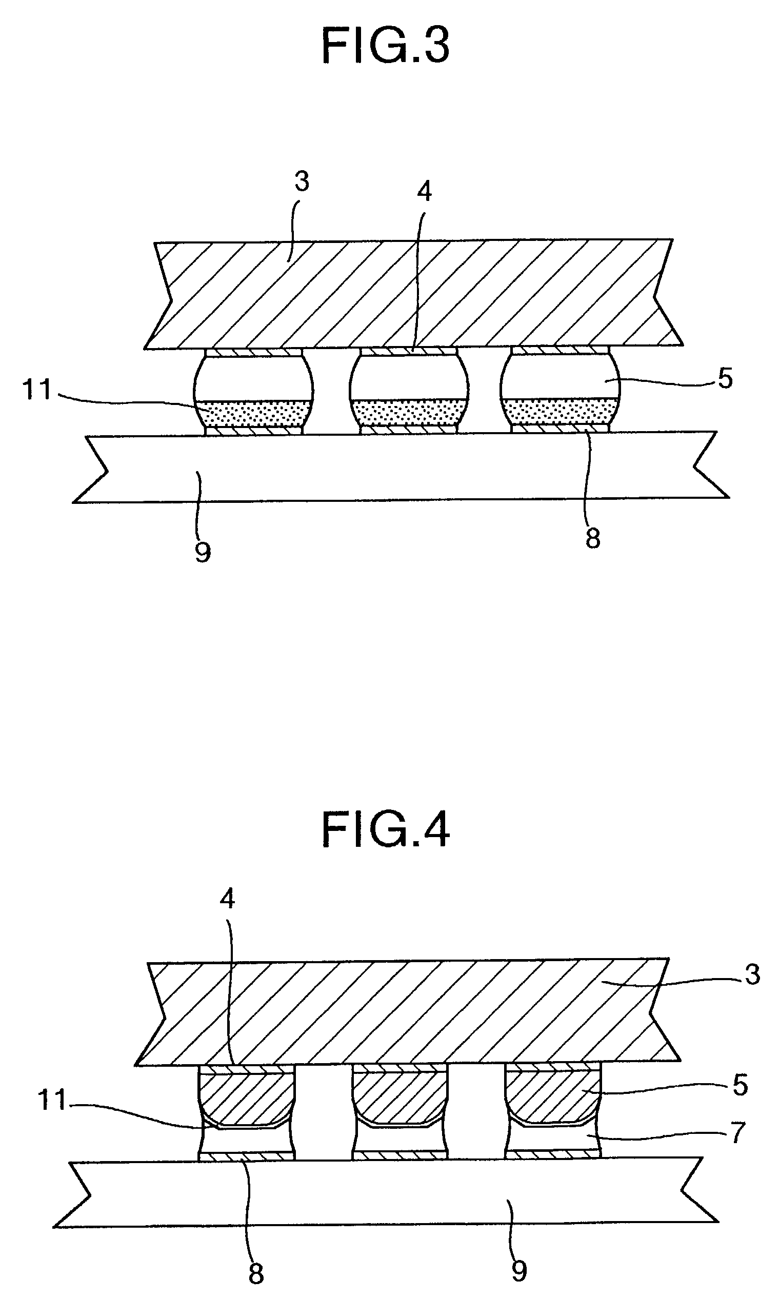
[0031]FIG. 1 a schematic view of an example of BGA used in the embodiment of the invention. The dimensions of a package used therein is 30 mm×30 mm, and a chip 2 located in the package has dimensions of 10 mm×10 mm. Each of solder bumps 5 has a diameter of 0.76 mm. Each of pads 4 formed on a BGA substrate 3 has a diameter of 0.6 mm, which pads are made of copper metallized with the plating layer of Ni (of a thickness of 10 to 25 μm) / Au (of a thickness of 0.5 to 1.2 μm). The mounting substrate 9 is FR-4 substrate having a thickness of 1 mm. Each of pads 8 provided on the substrate 9 has a diameter of 0.6 mm, each of the pads 8 being formed of copper metallized with the layer of Ni (of a thickness of 2 μm) / Au (of a thickness of 0.03 μm). The mounting thereof is performed by the steps of: transferring on the pads 8 a solder paste 7 through a printing mask which solder paste contains sol...


PUM

PropertyMeasurementUnit
Fractionaaaaaaaaaa
Fractionaaaaaaaaaa
Fractionaaaaaaaaaa

Abstract

A semiconductor module solder bonding of high reliability in which the heat resisting properties of the circuit substrate and electronic parts are taken into consideration. In order to achieve this, there are provided semiconductor devices each having solder bumps as external pads, and a circuit substrate bonded to the external pads of each of the semiconductor devices through a solder paste, each of the solder bumps being made of a first lead-free solder, the solder paste being made of a second lead-free solder having a melting point lower than that of the first lead-free solder.

Description

RELATED APPLICATION[0001]This application is a Continuation application of application Ser. No. 09 / 811,445, filed Mar. 20, 2001, now U.S. Pat. No. 6,486,411 issued Nov. 26, 2002, the contents of which are incorporated herein by reference in their entirety.BACKGROUND OF THE INVENTION[0002]The invention relates to a technique for mounting a semiconductor device.[0003]There is an increasing demand for semiconductor devices such as BGA, CSP, WPP, flip chip and etc. each of which semiconductor devices has bumps as external pads. In the semiconductor device having the bumps as the external pads, the bumps are formed by, for example, the steps of: preparing a pad pattern in which the plating of nickel-gold (Ni / Au) and nickel-palladium-gold (Ni / Pd / Au) is applied on the surface of copper; coating the pad pattern with flux by printing; mounting solder balls on the flux-coated pad pattern; and reflow-heating them so that the bumps may be formed.[0004]Further, the mounting of these semiconducto...

Claims


Application Information

Patent Timeline
IPC IPC(8): H01L23/48H01L21/48H05K3/34
CPCH05K3/3436H05K3/3463H05K2201/10992H01L2924/15311Y10T428/12715H01L2224/48227H01L2224/48091H01L2224/32225H01L2224/16225H01L2224/73204H01L2924/00014H01L2924/00H01L2224/05573H01L2224/05568H01L2224/05147H01L2224/05155H01L2224/05644H01L24/05Y02P70/50H01L23/12
Inventor MIURA, KAZUMASHIMOKAWA, HANAESERIZAWA, KOJISOGA, TASAONAKATSUKA, TETSUYA
Owner RENESAS ELECTRONICS CORP
Why Eureka
Try Eureka