Output overvoltage protection circuit for power amplifier

a protection circuit and power amplifier technology, applied in amplifier protection circuit arrangements, amplifiers with semiconductor devices only, amplifiers with semiconductor devices, etc., can solve the problems of thermal breakdown of the final-stage transistor, serious suffered from the aforementioned problem of transistor breakdown, and the inability to prevent thermal breakdown of the transistor, so as to reduce the output of the transistor

Active Publication Date: 2006-12-05
MURATA MFG CO LTD
View PDF14 Cites 71 Cited by
  • Summary
  • Abstract
  • Description
  • Claims
  • Application Information

AI Technical Summary

Benefits of technology

[0021]In view of the above circumstances, it is therefore an object of the present invention to provide a protection circuit for a power amplifier, which operates in response to an over output in an output-stage transistor to reduce the output of the transistor.
[0022]In order to achieve the above object, according to the present invention, there is provided an output overvoltage protection circuit for a power amplifier, including a monitor circuit for monitoring an output overvoltage of an output transistor in either one of a plurality of stages (preferably, the final stage) of the power amplifier and allowing a current to flow therethrough in response to the monitored output overvoltage, and a current mirror circuit for supplying a current proportional to the current from the monitor circuit in such a manner that the base bias of the first-stage transistor of the power amplifier is reduced in response to the current supplied from the current mirror circuit, to reduce the output of the final-stage output transistor.
[0023]According to the present invention, in response to the monitored output overvoltage of the transistor in either one of the stages (preferably, the final stage) of the power amplifier, the bias of the first-stage transistor is reduced to control the output of the power amplifier. Thus, if an over output is generated in the final-stage transistor due to load change in power-supply overvoltage conditions, the bias of the first-stage transistor can be controlled to immediately suppress the over output of the final-stage transistor so as to avoid the risk of thermal breakdown in the final-stage transistor.

Problems solved by technology

Consequently, if a load impedance is changed to a value far greater than a usual value of 50 Ω when a power supply voltage is increased to a value (e.g. 4.5 V to 5.5 V) greater than a recommended operating condition (3 V to 3.6 V) during battery charge, a load curve of a final-stage transistor will be significantly changed, resulting in thermal breakdown of the final-stage transistor.
Therefore, portable telephone systems, such as GSM, where the fluctuation or change in power supply voltage or load has direct impact on a power amplifier have seriously suffered from the aforementioned problem of transistor breakdown.
Thus, these techniques cannot prevent thermal breakdown of the transistor due to over output of the transistor itself

Method used


Image

  • Output overvoltage protection circuit for power amplifier
  • Output overvoltage protection circuit for power amplifier
  • Output overvoltage protection circuit for power amplifier

Examples


first embodiment

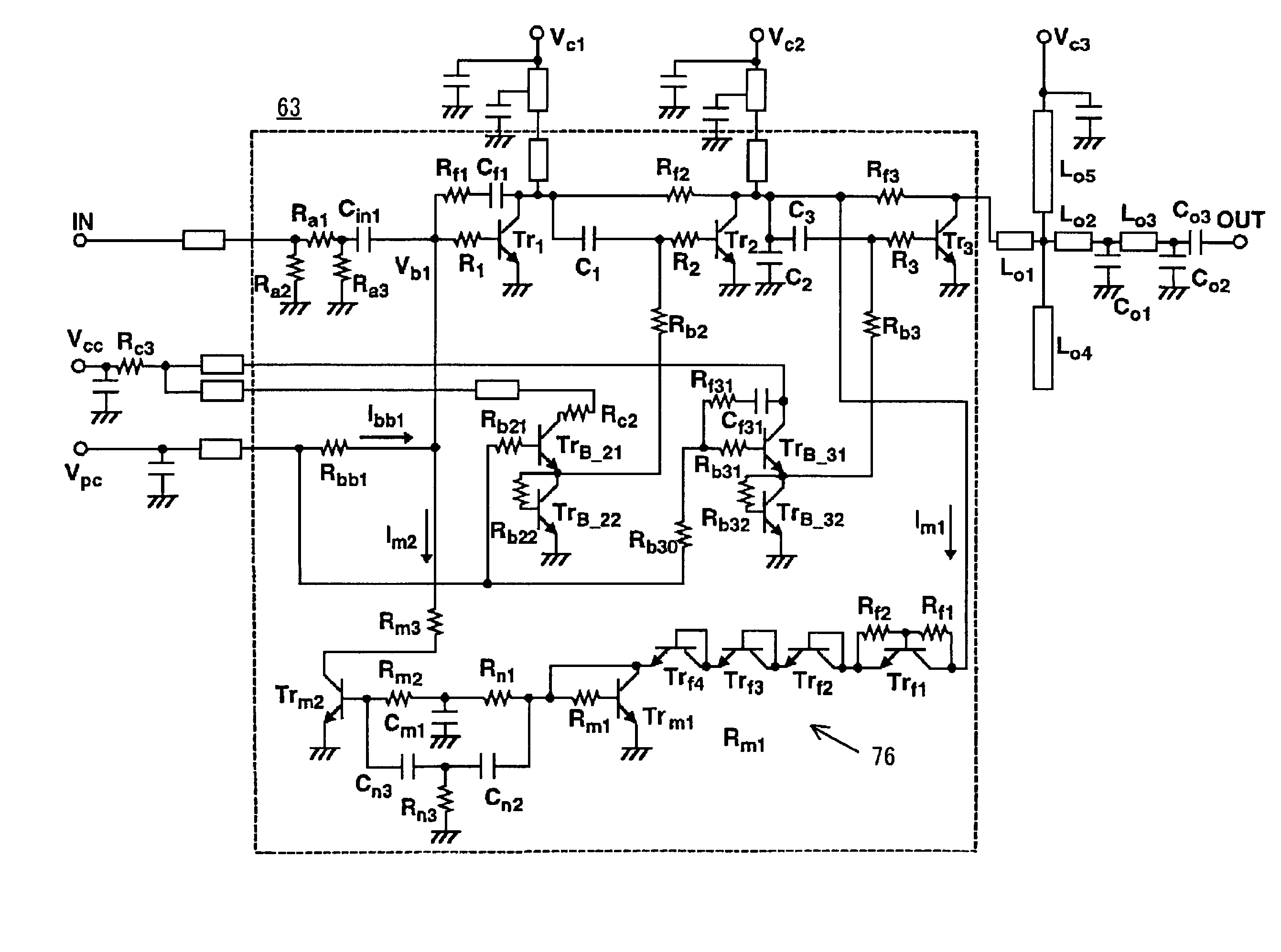
[0042]FIG. 1 shows a circuitry of a GSM power amplifier with an output overvoltage protection circuit according to a first embodiment of the present invention. A signal entered into an input terminal IN is amplified through three amplifier HBTs (hereinafter referred to as “transistors”) Tr1 to Tr3 in this order. A voltage Vpc supplied to an output-power control terminal acts to supply a base current (bias) to the transistor Tr1 and to supply a base current to the transistors Tr2, Tr3, respectively, through transistors (TrB_21, TrB_22) and transistors (TrB_23, TrB_24) which are fed from an voltage Vcc at a power supply terminal, so as to variably control the output of the final-stage transistor Tr3. The output of the final-stage transistor Tr3 is led to an output terminal OUT through microwave lines Lo 1 to Lo 5.

[0043]Each of the transistors Tr1 to Tr3 has characteristics of providing a high low-frequency gain, and easily oscillating at a low frequency as compared to a FET power ampl...

second embodiment

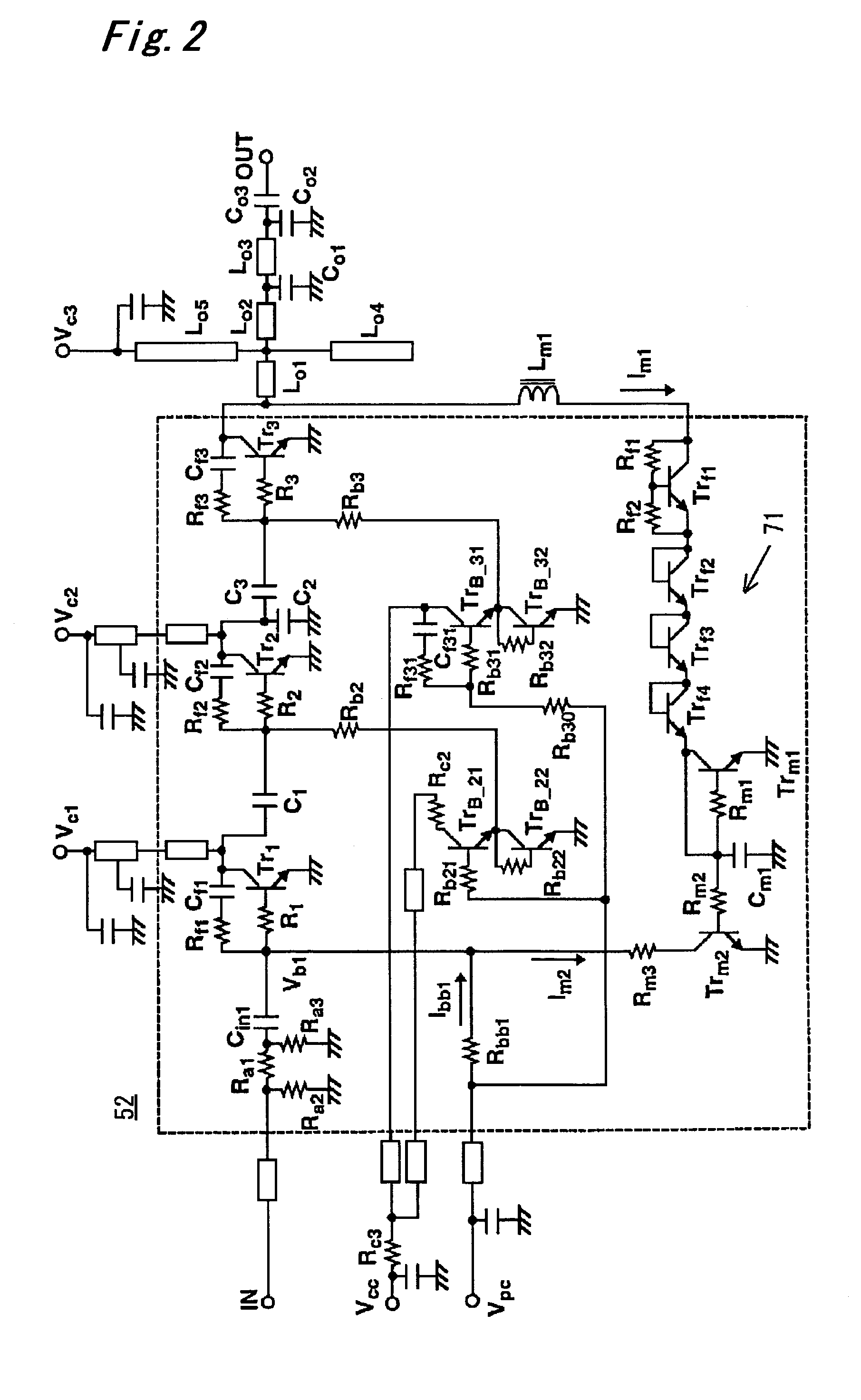
[0054]FIG. 2 shows a power amplifier 52 with an output overvoltage protection circuit according a second embodiment of the present invention. In addition to the circuitry in FIG. 1, the power amplifier 52 includes an RF blocking inductor Lm1 inserted into a line connecting between the collector of the final-stage transistor Tr3 and the collector of the transistor Trf1 in the output-voltage feedback section.

[0055]In the circuitry of FIG. 1, if the voltage smoothing in the current mirror section is not sufficient, ripples to be varied according to operating frequencies will be included in the current I m2. This creates a parasitic oscillation loop such that the bias of the first-stage transistor Tr1 is slightly changed and this slight change causes a subtle change in the output voltage.

[0056]In particular, when the power amplifier has a high small signal gain, the above parasitic oscillation becomes significant. Therefore, it is required to design the power amplifier while sufficientl...

third embodiment

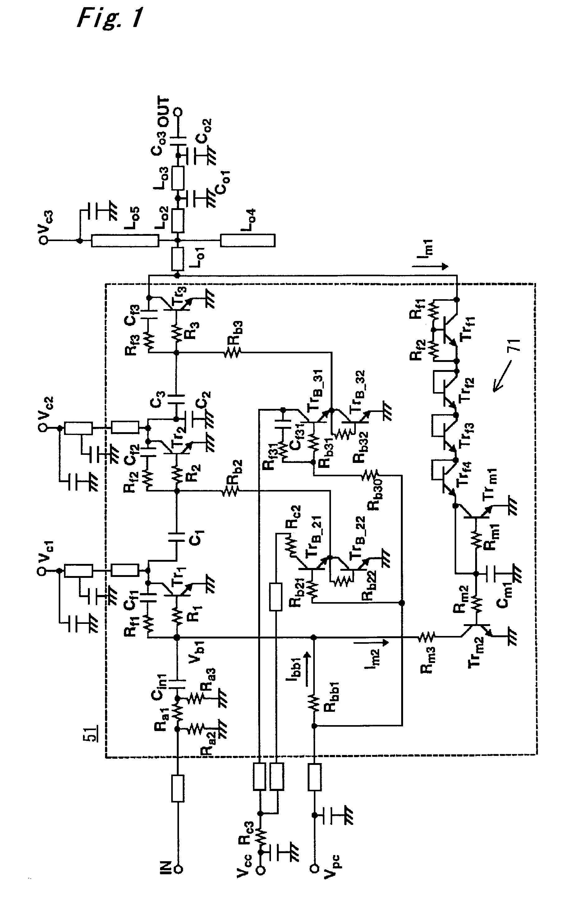
[0057]As with the second embodiment, a protection circuit according to a third embodiment is directed to suppress the parasitic oscillation. While the circuitry in FIG. 1 is configured such that the feedback output from the transistor Trm2 in the feedback circuit is fed back directly to the feedback section of the first-stage transistor Tr1, the feedback output is fed back through a resistor Rbb2 in a power amplifier 53 in FIG. 3 illustrating the third embodiment.

[0058]This configuration can reduce ripples included in the current I m2 to suppress the parasitic oscillation as with the second embodiment. This protection circuit also has the same effects as those in the first embodiment.


PUM


Abstract

Disclosed is an output overvoltage protection circuit for a power amplifier having a plurality of stages, which comprises a monitor circuit for monitoring an output overvoltage of an output transistor in the final stage of the power amplifier and allowing a current to flow therethrough in response to the monitored output overvoltage, and a current mirror circuit for supplying a current proportional to the current from the monitor circuit in such a manner that the base bias of the first-stage transistor of the power amplifier is reduced in response to the current supplied from the current mirror circuit, to reduce the output of the final-stage output transistor.

Description

BACKGROUND OF THE INVENTION[0001]1. Field of the Invention[0002]The present invention relates to a power amplifier, such as GaAs HBT or Si bipolar transistor power amplifier, and more particularly to a protection circuit for preventing the breakdown of an output-stage transistor of a power amplifier during load change (during output load mismatch) in output overvoltage conditions.[0003]2. Description of the Related Art[0004]In power amplifiers for mobile communication, a GaAs MESFET, GaAs HEMT and GaAs-based HBT are expected as future power elements for mobile communication, by reason that they have the following advantages as compared to a conventional FET:[0005](1) Capability of single power-supply operation because of no need for negative gate bias voltage;[0006](2) Capability of ON / OFF operation without any analog switch on drain side as with a Si-MOSFET; and[0007](3) Capability of providing high output current density and facilitating the reduction in size required for obtainin...

Claims


Application Information

Patent Timeline
Patent Type & Authority Patents(United States)
IPC IPC(8): H03F1/52H03F3/21
CPCH03F1/52
Inventor YAMAMOTO, KAZUYASHIMURA, TERUYUKIASADA, TOMOYUKISUZUKI, SATOSHI
Owner MURATA MFG CO LTD
Why Eureka
Try Eureka