

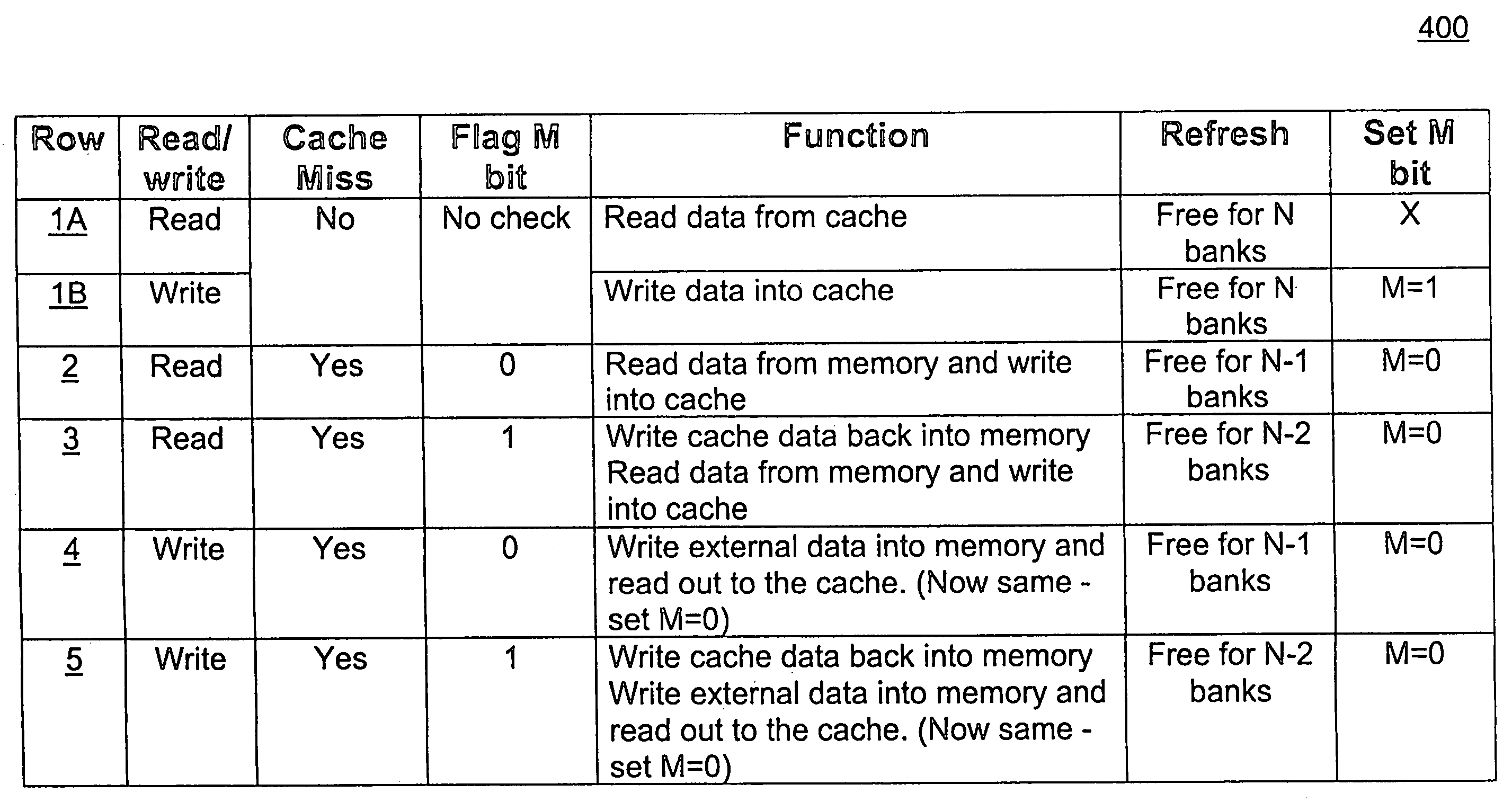
Hiding refresh in 1T-SRAM architecture
a technology of sram and refresh operation, applied in the field of semiconductor memories, can solve the problems of inefficiency, intransparent refresh operation, and limited success of previous attempts to use dram cells in sram applications
- Summary
- Abstract
- Description
- Claims
- Application Information
AI Technical Summary
Benefits of technology
Problems solved by technology
Method used
Image

Examples
Embodiment Construction
[0026]In the following detailed description of the embodiments, numerous specific details are set forth in order to provide a thorough understanding of the present invention. However, it will be recognized by one skilled in the art that the present invention may be practiced without some specific details or with equivalents thereof. In other instances, well-known methods, procedures, components, and circuits have not been described in detail as not to unnecessarily obscure aspects of the embodiments.
[0027]Some portions of the detailed descriptions which follow are presented in terms of procedures, steps, logic blocks, processing and other symbolic representations of operations on data bits that can be performed on computer memory systems. These descriptions and representations are the means used by those skilled in the data processing arts to most effectively convey the substance of their work to others skilled in the art. A procedure, computer executed step, logic block, process, e...
PUM
 Abstract
Description
Claims
Application Information