Plastic semiconductor package having improved control of dimensions

Active Publication Date: 2006-12-12
TEXAS INSTR INC
View PDF7 Cites 26 Cited by
  • Summary
  • Abstract
  • Description
  • Claims
  • Application Information

AI Technical Summary

Benefits of technology

[0011]It is a technical advantage that the invention provides thin devices free of any voids and having unusually flat surfaces and high luster. Furthermore, the production throughput is about an order of magnitude higher compared to conventional potting encapsulation.
[0012]It is another technical advantage that the invention can b

Problems solved by technology

Foremost, the process is hard to control uniformly and prone to statistical variations such as uneven fillings, pronounced meniscus formation, or flaws such as voids.
The choice of materials is limited to semi-liquid materials which typically require prolonged “curing” times for polymerization and hardening, causing high mechanical stress in the product.
Secondly, the existing technology process is not economical.
In order to keep the number of dispensers in practical limits, only a modest number of packages

Method used


Image

  • Plastic semiconductor package having improved control of dimensions
  • Plastic semiconductor package having improved control of dimensions
  • Plastic semiconductor package having improved control of dimensions

Examples


Example

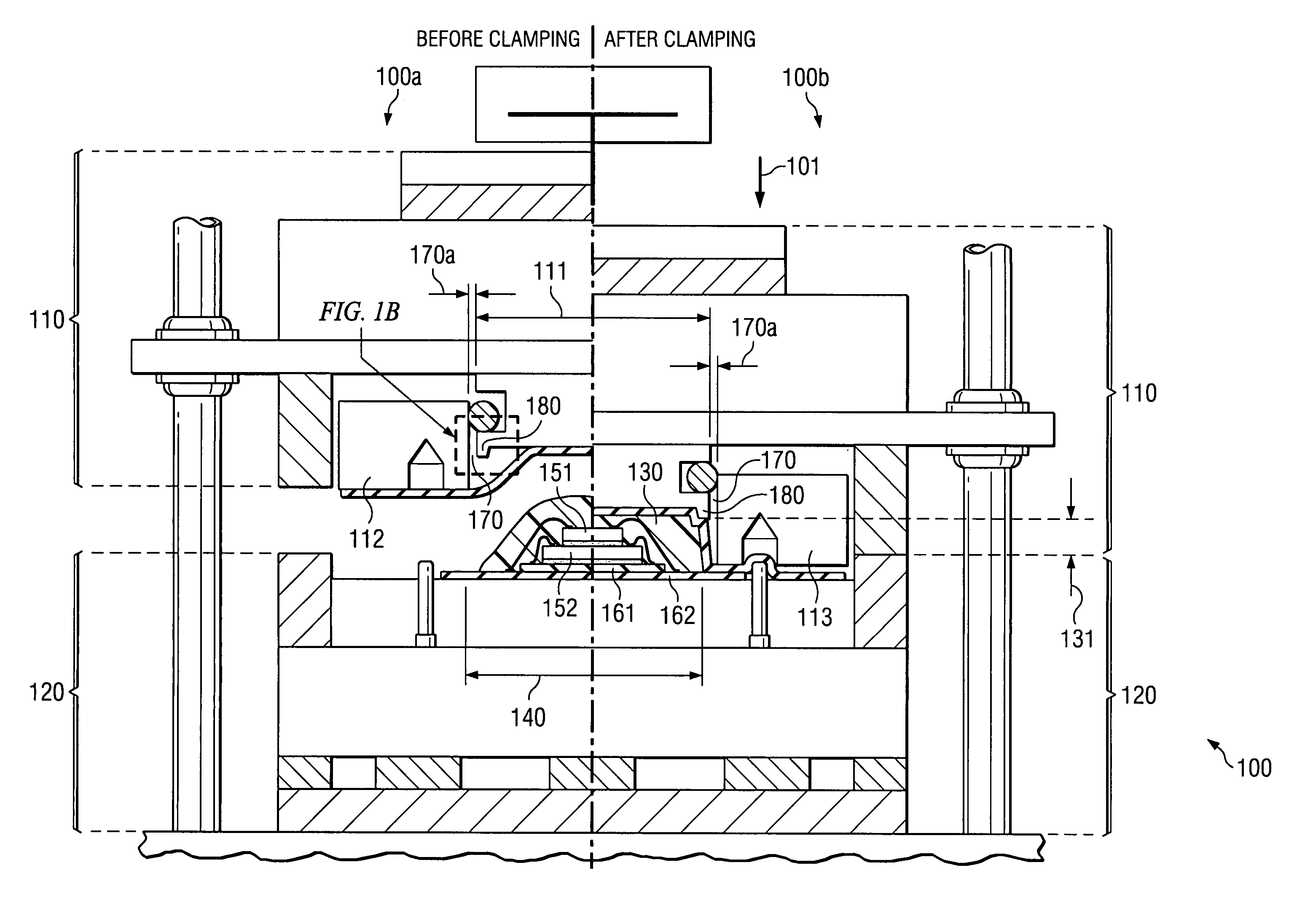
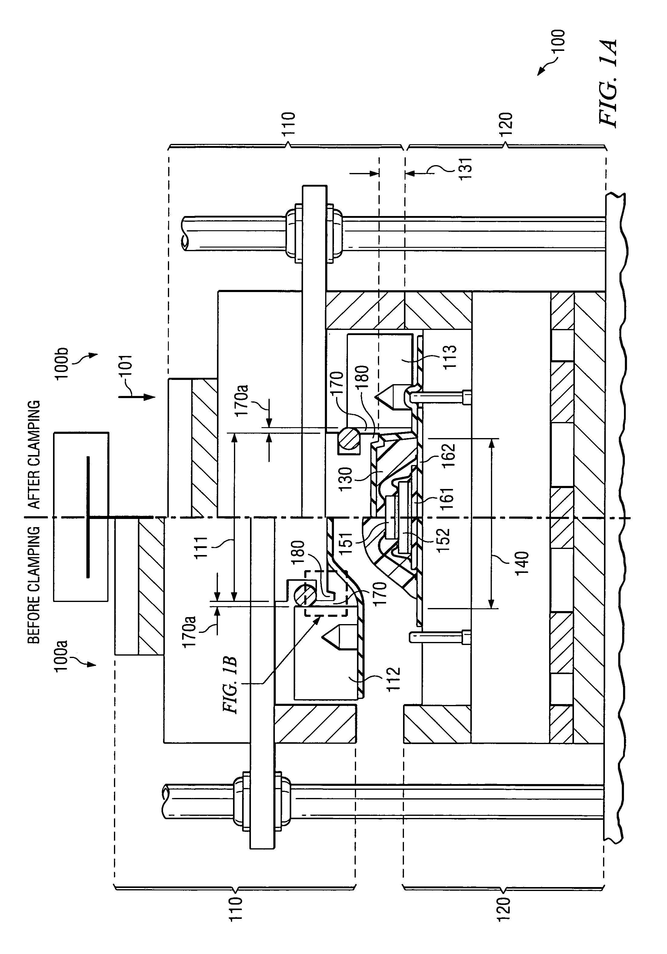
[0027]FIG. 1A depicts an apparatus, generally designated 100, for packaging a device, especially a semiconductor device, according to one embodiment of the invention. The package of the device is intended to have a planar top area and planar side areas. The apparatus of FIG. 1A is designed for the compression molding technique as the preferred technology to utilize the innovations of the invention. It should be stressed, however, that an apparatus suitable for a transfer molding technique or a potting technique may also incorporate features of the invention. The left hand portion 100a of the apparatus in FIG. 1A illustrates the apparatus before the process step of clamping, the right hand portion 100b illustrates the apparatus after the process step of clamping, whereby the direction of the clamping step is indicated by the arrow 101. An apparatus for the compression molding technique, which can be fitted with a top mold embodying this invention as shown in FIG. 1A, is commercially ...


PUM

PropertyMeasurementUnit
Fractionaaaaaaaaaa
Fractionaaaaaaaaaa
Areaaaaaaaaaaa

Abstract

A device with a semiconductor chip (801) assembled on a planar substrate (802) and encapsulation compound (810) surrounding the assembled chip and a portion of the substrate near the chip; the compound has a planar top area (811). The encapsulation compound has a plurality of side areas (812) reaching from the substrate to the top area; these side areas form edge lines with the top area, where the top area plane intersects with the respective plane of each side area. The encapsulation compound is recessed (813) along the edge lines so that the material is caved-in along the lines; this feature causes the recess to prevent any compound from the side area planes to reach the top area plane, whereby the planarity of the top area is preserved.

Description

FIELD OF THE INVENTION[0001]The present invention is related in general to the field of semiconductor devices and processes and more specifically to encapsulation methods for integrated circuit chips resulting in thin and substantially flat packages having improved control of dimensions and board assembly properties.DESCRIPTION OF THE RELATED ART[0002]During the last few years, a major trend in the semiconductor industry has been the effort to shrink semiconductor packages so that the package outline consumes less area and less height when it is mounted onto customer circuit boards, and to reach these goals with minimum cost (both material and manufacturing cost). One of the most successful approaches has been the development of so-called “chip-scale packages”. These packages have an outline adding less than 20% to the chip area. A chip-scale package which has only the outline of the chip itself is often referred to as “chip-size package”.[0003]The process of encapsulating ship-scal...

Claims


Application Information

Patent Timeline
IPC IPC(8): H01L21/56B29C45/14
CPCB29C43/18B29C43/36H01L21/565H01L21/566B29C2043/3626H01L2224/48091H01L2224/48227H01L2924/15311H01L2924/1815H01L2924/00014H01L2224/32225H01L2224/73265H01L2924/00012H01L2924/00H01L24/73H01L2924/14H01L2224/32145H01L21/56B29C70/72B29C45/14
Inventor TAKAHASHI, YOSHIMI
Owner TEXAS INSTR INC
Why Eureka
Try Eureka