
Process-oriented modulized plant for TFT-LCD fabrication

a technology of process-oriented modulation and tft-lcd, which is applied in the direction of non-linear optics, instruments, coatings, etc., can solve the problems of deterioration of the yield rate of the fabrication, the construction schedule and safety problems of the plant with preset invention are well under control, and the cross contamination between processes of variable environmental requirements can be prevented, and the cost of whole-plant expenses can be reduced.

Inactive Publication Date: 2006-12-12
L&K ENG
View PDF4 Cites 1 Cited by
  • Summary
  • Abstract
  • Description
  • Claims
  • Application Information

AI Technical Summary

Benefits of technology

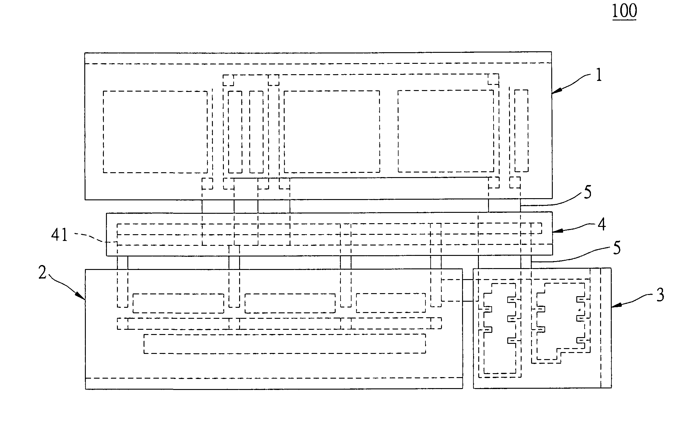
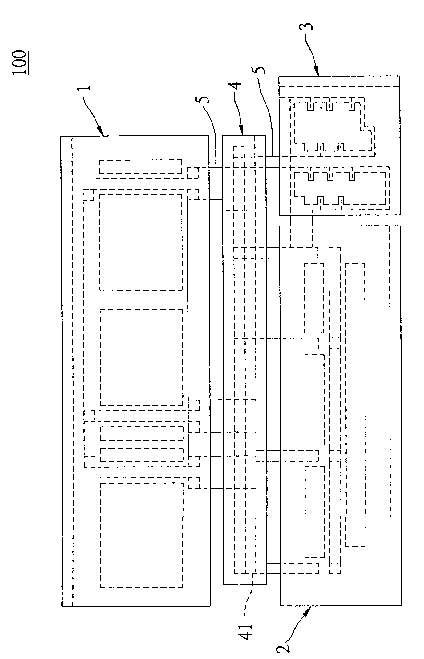
[0016]An object of the present invention is to provide a process-oriented modulized plant for TFT-LCD fabrication, which includes a plurality of individual fabs. The individual fabs independent to others are capable of preventing the cross contaminations. In addition, the processes are based on environmental requirements as to be carried out in different fabs. At least one process locates in each fab, which can be treated as one module. Thus, the cross contaminations between processes of variable environmental requirements can be prevented, the whole-plant expenses can be reduced and the damages by fire accident or smoke pollution can be avoided. If a fire accident were to happen, the plant according to the present invention would be recovered within short reconstruction time and low reconstruction expenses. Furthermore, the construction costs can be saved by setting up the fabs at properly classified levels of microvibration control. In addition, the construction schedule and safety problems of plants with preset invention are well under control.
[0017]Another object of the present invention is to provide a process-oriented modulized plant for TFT-LCD fabrication, including automatic transport-and-storage systems for central collection and distribution, setting up in respective warehouses. The warehouses are located between these fabs so that the height of fabs can be reduced.

Problems solved by technology

In addition, the construction schedule and safety problems of plants with preset invention are well under control.
The second independent fab carries out at least another process, which is affected by the contamination from the first group of contaminants, results in deterioration of yield rate of the fabrication.

Method used


Image

  • Process-oriented modulized plant for TFT-LCD fabrication
  • Process-oriented modulized plant for TFT-LCD fabrication

Examples


Embodiment Construction

[0022]According to the present invention, a process-oriented modulized plant for TFT-LCD fabrication is provided in the FIGURE.

[0023]A plant 100 for manufacturing TFT LCD includes a thin film process, a photolithography process, an etching process and a stripping process.

[0024]The thin film process is a high heat-releasing process with a low cleanliness requirement (FED Std 209E Class 10,000), and is affected by contaminations of organic or acidic gases. In other words, the thin film process is sensitive to the corresponding contaminants from the other fabs that can generate organic or acidic gases.

[0025]The photolithography process is influenced by microvibrations, temperature and humidity (i.e., sensitive to microvibrations, temperature and humidity). The photolithography process has a high cleanliness requirement (FED Std 209E Class 100 or Class 10), and is a source of organic gases. In other words, the photolithography process is an organic-gas contamination source.

[0026]The etc...


PUM

PropertyMeasurementUnit
temperature/humidityaaaaaaaaaa
yield rateaaaaaaaaaa
defectsaaaaaaaaaa

Abstract

A process-oriented modulized plant for TFT-LCD fabrication capable of preventing cross contaminations is proposed. A plant includes a plurality of independent fabs and warehouses connected between the fabs. Each independent fab can carry out at least one TFT-LCD processes. The respective process used in the first independent fab produces the first group of contaminants. Another respective processes carried out in the second independent fab are affected by the contaminations from the first group of contaminants and results in deterioration of yield rate of the fabrication. At least one automatic transport-and-storage system for central collection and distribution is located in each warehouse. Each warehouse is connected to the independent fabs via at least one automated material handling system to link up the processes together. Moreover, the processes carried out in these independent fabs differ from the others, generate different contamination sources, and / or are sensitive to the corresponding sources form the others.

Description

BACKGROUND OF THE INVENTION[0001]1. Field of the Invention[0002]The present invention relates to a process-oriented modulized plant for TFT-LCD fabrication and that is capable of modulizing fabs corresponding to the characteristics of the manufacturing processes. The modulized plant is provided to avoid cross contaminations between the processes.[0003]2. Description of Related Art[0004]As the TFT-LCD technology progresses, particulates are no longer the main factor that causes defects of microelectronic devices and circuits. The cross contaminations existing between different processes have gradually become another important factor that causes the defects. For example, the thin film process is subject to the contamination of organic or acid gases, which affect the yield, yet the photolithography process produces these organic gases. Moreover, the photolithography process is influenced by temperature, humidity, and microvibrations that may lower the yield, but the thin film process i...

Claims


Application Information

Patent Timeline
Patent Type & Authority Patents(United States)
IPC IPC(8): G06F19/00
CPCG02F1/1303H01L21/67161H01L21/67727H01L27/1214
Inventor YAO, KENNETH
Owner L&K ENG
Learn More