Anodic bonding method and electronic device having anodic bonding structure

Inactive Publication Date: 2006-12-26
HITACHI LTD
View PDF7 Cites 39 Cited by
  • Summary
  • Abstract
  • Description
  • Claims
  • Application Information

AI Technical Summary

Benefits of technology

[0016]According to the technique employed in accordance with the present invention, good close adhesion can be attained for a glass layer and a conductor layer or a semiconductor layer at a lower bonding temperature than usual, and bonding which is firm also from a chemical point of view can be obtained by use of an active metal. As a means of obtaining good close adhesion, a soft metal layer is disposed on the surface of a conductor or semiconductor. Thus, when the glass and the conductor or semiconductor are attracted to each other by an electrostatic attraction force, even in a case where dust or undulations are present on the boundary, the soft metal layer is deformed so as to provide good close adhesion. In a case of using Sn or Pb, or when an alloy containing them is used, as the soft metal layer, they may be possibly melted during bonding. However, even when they are melted, since a pure metal layer containing at least one of

Problems solved by technology

However, in case it is intended to bond a Si wafer at a temperature, for example, of 300° C. or lower, such molten eutectics cannot be formed.
When the solder at the d

Method used


Image

  • Anodic bonding method and electronic device having anodic bonding structure
  • Anodic bonding method and electronic device having anodic bonding structure
  • Anodic bonding method and electronic device having anodic bonding structure

Examples


first embodiment

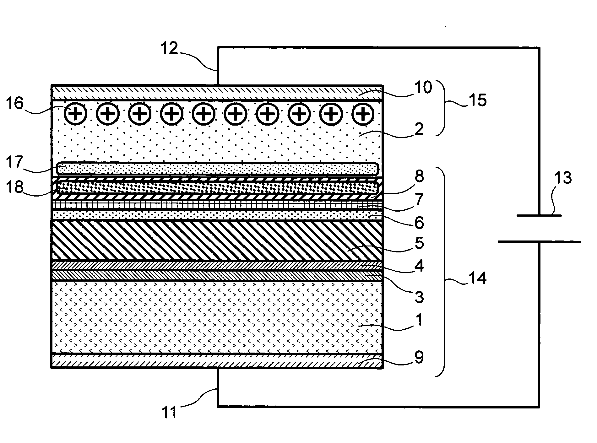
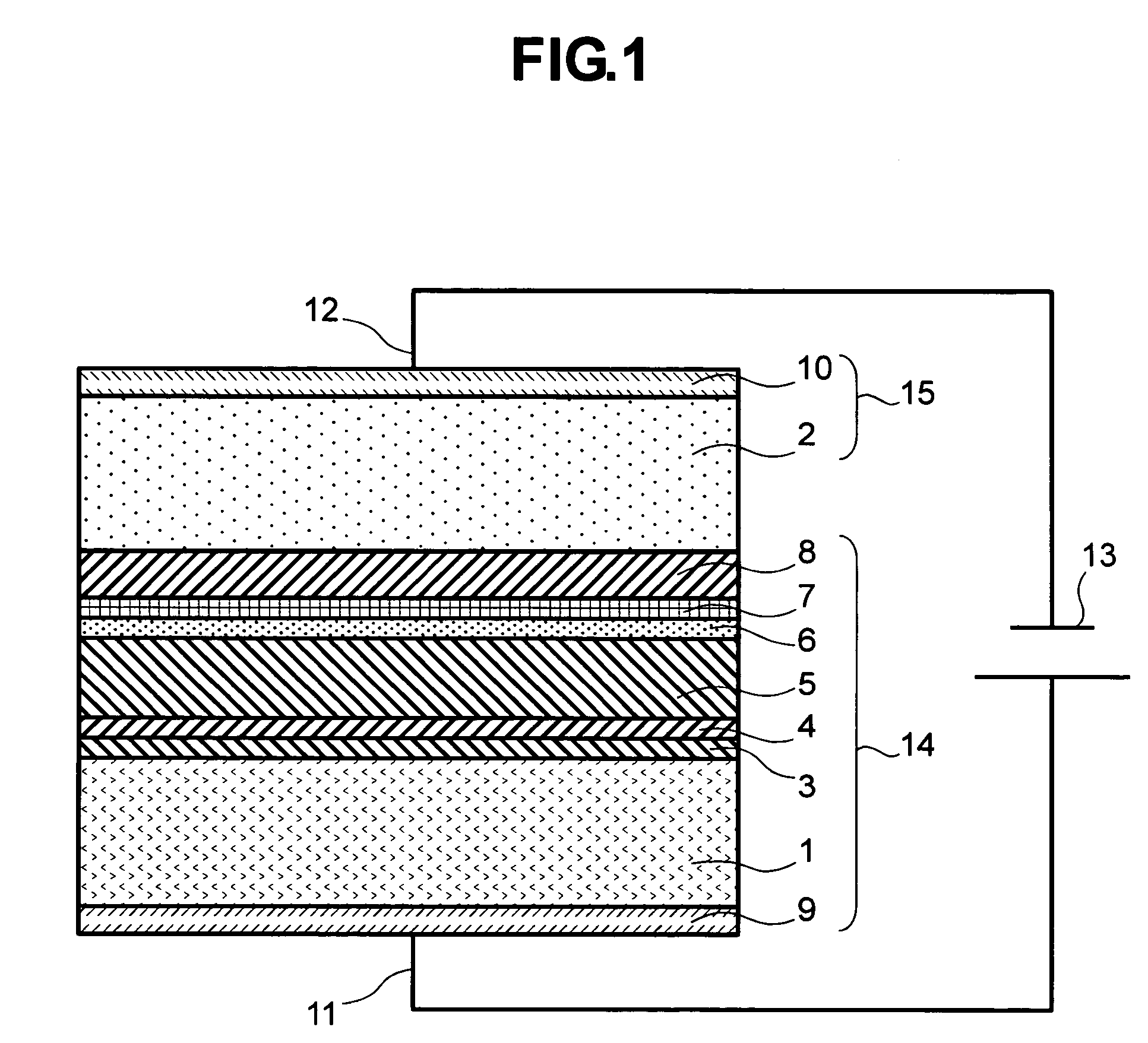
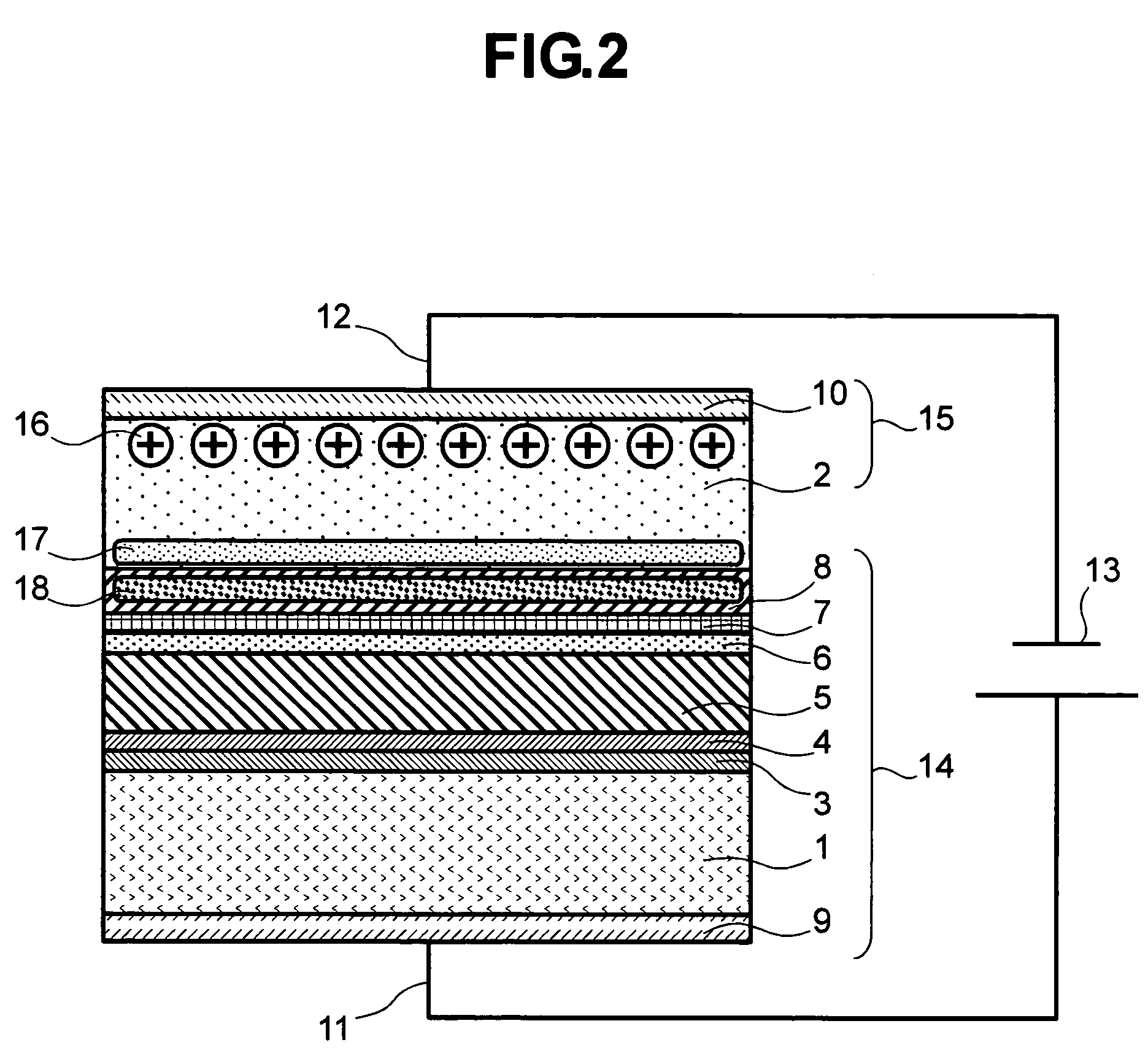
[0028]the invention will be described with reference to FIG. 1. On a Si layer 1, a Ti film 3, a Pt film 4 and an Au film 5 are formed by vacuum vapor deposition or sputtering. The Ti film 3 has a function of improving the adhesion with the Si layer 1. The Pt film 4 has a function of improving the adhesion between the Au film 5 and the Ti film 3. The Au film 5 has a function, as a soft metal layer, of improving the adhesion with glass through deformation at the time of anodic bonding. The description of this embodiment makes reference by way of example to the use of Au as a representative of the type of soft metal that may be employed, but the soft metal layer is not restricted to the use of Au. Although, depending on the bonding temperature, Au, Ag, Cu, Pb or Sn is extremely soft even at a temperature of about 200° C. and shows sufficient deformation. Accordingly, in a case of using such a soft metal, it can be deformed sufficiently even if dust or wafer undulations are present more...

fourth embodiment

[0038]the invention will be described with reference to FIG. 6. A stack of an Au film 5 and an Sn film 20 is used as the soft metal layer. When the stack is heated at a bonding temperature of, e.g., 300° C., the Sn film 20 is melted, and, immediately thereafter, the Al film 8, the Ti film 7 and the Pt film 6 are deformed in such a manner as to conform the surfaces of inclusions and the glass 2. Subsequently, diffusion of cations in the glass is promoted by the application of voltage for anodic bonding. During heating, the Sn film 20 is instantly diffused into the Au film 5 to form an Au—Sn alloy. If the original thickness of the Au film 5 and the Sn film 20 is designed for the Au—Sn alloy such that the average composition has an Sn concentration of Au-12% Sn or less, the portion is not melted even when heated at 280° C. or higher in the subsequent process. That is, the film is melted temporarily in order to obtain good adhesion upon anodic bonding, and then the melting point is made...

fifth embodiment

[0039]the invention will be described with reference to FIG. 7. Metal films 23 for anodic bonding are provided in such a manner as to be connected to a lens 24 at portions other than at a light transmission portion 30 of the lens 24. An anode film 26 at the lower surface of a Si bench 21 may be provided over the entire surface of the Si bench 21 with no problem depending on the bonding conditions. However, if it is located at a position corresponding to the position of the metal film 23 at the back surface of the Si bench 21 and a cathode film 25 on the side of the lens 24 is also located at a position corresponding to the position of the metal film 23, while a DC voltage is concentratedly applied to this portion, and diffusion of ions in the lens 24 is restricted to a portion other than the light transmission portion. Accordingly, mounting can be performed while avoiding the effect of a delicate change of the refractive index caused by the diffusion of ions in the lens.

[0040]In the...


PUM

PropertyMeasurementUnit
Temperatureaaaaaaaaaa
Structureaaaaaaaaaa
Adhesion strengthaaaaaaaaaa

Abstract

In anodic bonding between a conductor or semiconductor and glass, in order to attain good adhesion at a lower bonding temperature than usual and improve the toughness at its boundary to obtain higher reliability for a bonded portion even in a case where bonded members are warped or dust is present at the bonding boundary, a soft metal film is formed on the surface of a conductor or semiconductor on which an active metal film having high reactivity with oxygen is formed, whereby a warp or dust, if any, can be absorbed by the deformation of the soft metal film, thereby to improve the adhesion at the boundary. Adhesion at the bonding boundary is improved even at a low bonding temperature of, e.g., about 200° C. Further, the toughness at the bonding boundary can be improved to increase reliability by roughening the bonded surface on the side of the glass.

Description

CROSS REFERENCE TO RELATED APPLICATION[0001]The disclosure of Japanese Patent Application No. JP2003-053410, filed on Feb. 28, 2003, including the specification, drawings and abstract thereof, is incorporated herein by reference in its entirety.BACKGROUND OF THE INVENTION[0002]The present invention relates to an electronic device having an anodic bonding structure consisting of a conductor or semiconductor and glass; and, more particularly, the invention relates to a micro-machine technique, including the use of micro-sensors and micro-pumps, and to an optical component.[0003]Since anodic bonding can be employed to directly bond a semiconductor, such as Si, and glass, it is used mainly in the field of MEMS (Micro Electro Mechanical Systems) for the manufacture of micro-mechanical components by fabrication of Si. Since the principle of anodic bonding is reported in a significant amount of literature, such as Japanese Patent Laid-open No.10-259039, only an outline thereof will be desc...

Claims


Application Information

Patent Timeline
IPC IPC(8): H01L21/326B32B37/00C03C27/00C03C27/02H01L21/20H01L29/84
CPCC03C27/00C03C27/02H01L21/2007
Inventor HATA, SHOHEISOTOKAWA, HIDEOFURUICHI, HIROAKI
Owner HITACHI LTD
Why Eureka
Try Eureka