
Organic photovoltaic cells with an electric field integrally-formed at the heterojunction interface

a photovoltaic cell and heterojunction technology, applied in the field of photovoltaic cells and semiconductors, can solve the problems of recombination, high dollar and environmental costs associated with manufacturing of inorganic solar cells, and increasing costs and shortages of more standard energy sources

Inactive Publication Date: 2007-01-02
ALLIANCE FOR SUSTAINABLE ENERGY
View PDF8 Cites 38 Cited by
  • Summary
  • Abstract
  • Description
  • Claims
  • Application Information

AI Technical Summary

Benefits of technology

This approach enhances solar conversion efficiency by up to 5% or more, addressing recombination issues and adhesion problems, while enabling the use of flexible and durable organic solar cells with improved light absorption and reduced material costs.

Problems solved by technology

The conversion of solar energy into electrical energy is becoming more important as costs and shortages of more standard energy sources continue to increase.
While relatively efficient, inorganic solar cells often have high dollar and environmental costs associated with manufacturing as the cells are made of toxic materials that typically have to be grown as a single large crystal.
Unfortunately, the solar conversion efficiencies of existing organic solar or photovoltaic (PV) cells is typically less than 10 to 20 percent of the solar conversion efficiencies obtainable in inorganic PV cells or in some cases, only 1 to 2 percent conversion efficiency.
However, due to the differences in the dissociation mechanisms of OPV and IPV cells, recombination is a particular problem at the interface in OPV cells.
Recombination is a larger problem at the interface in OPV cells due to the much larger concentration of carriers at the interface when compared to IPV cells in which the carriers are distributed in the bulk.
This is an effective approach for IPV cells in which the electrons can only be separated from the holes by applying such an electrical potential-energy gradient, but application of a uniform electric field across the bulk has not proven effective in OPV cells where a critical efficiency limitation is recombination at the interface of the two semiconductor layers.
Unfortunately, doping of organic materials is a difficult and often impractical process that has not addressed the low efficiency issues in OPV cells.
One difficulty with doping in OPV cells is that the integrity of the organic semiconductor materials are often chemically or morphologically disturbed, which can create exciton traps or quenching cites that block diffusion and / or cause recombination.
However, single crystals of organic semiconductors generally cannot be used for devices, such as for OPV cells, because the crystals are quite small, i.e., 0.1 to 10 μm, and do not adhere well to most substrates or to other organic semiconductors.
This lack of good adhesion is a problem that must be addressed in manufacturing an OPV cell because good crystal-to-crystal contact is required throughout the cell to maintain electron and hole paths.
When the conventional method of sublimation is used to apply organics to a surface, the resulting film is commonly amorphous or nanocrystalline but is usually not strongly adherent and often causes serious interfacial adhesion problems.
Attempts have been made to address this problem with annealing by heating or exposing the films to a solvent vapor, but to date, the resulting crystalline films have had numerous pinholes that have led to semiconductor devices with unacceptable electrical shorts.

Method used


Image

  • Organic photovoltaic cells with an electric field integrally-formed at the heterojunction interface
  • Organic photovoltaic cells with an electric field integrally-formed at the heterojunction interface
  • Organic photovoltaic cells with an electric field integrally-formed at the heterojunction interface

Examples


Embodiment Construction

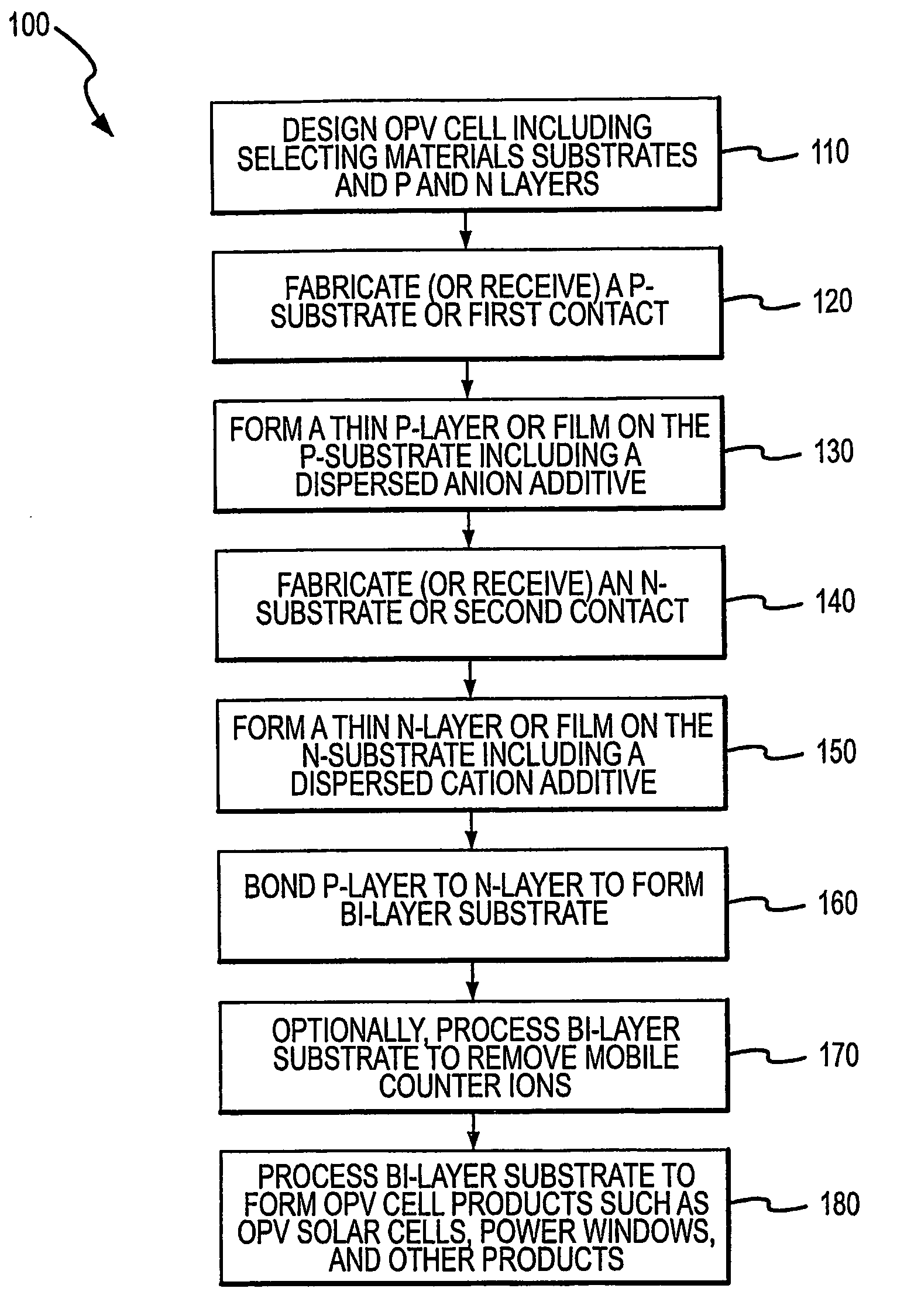
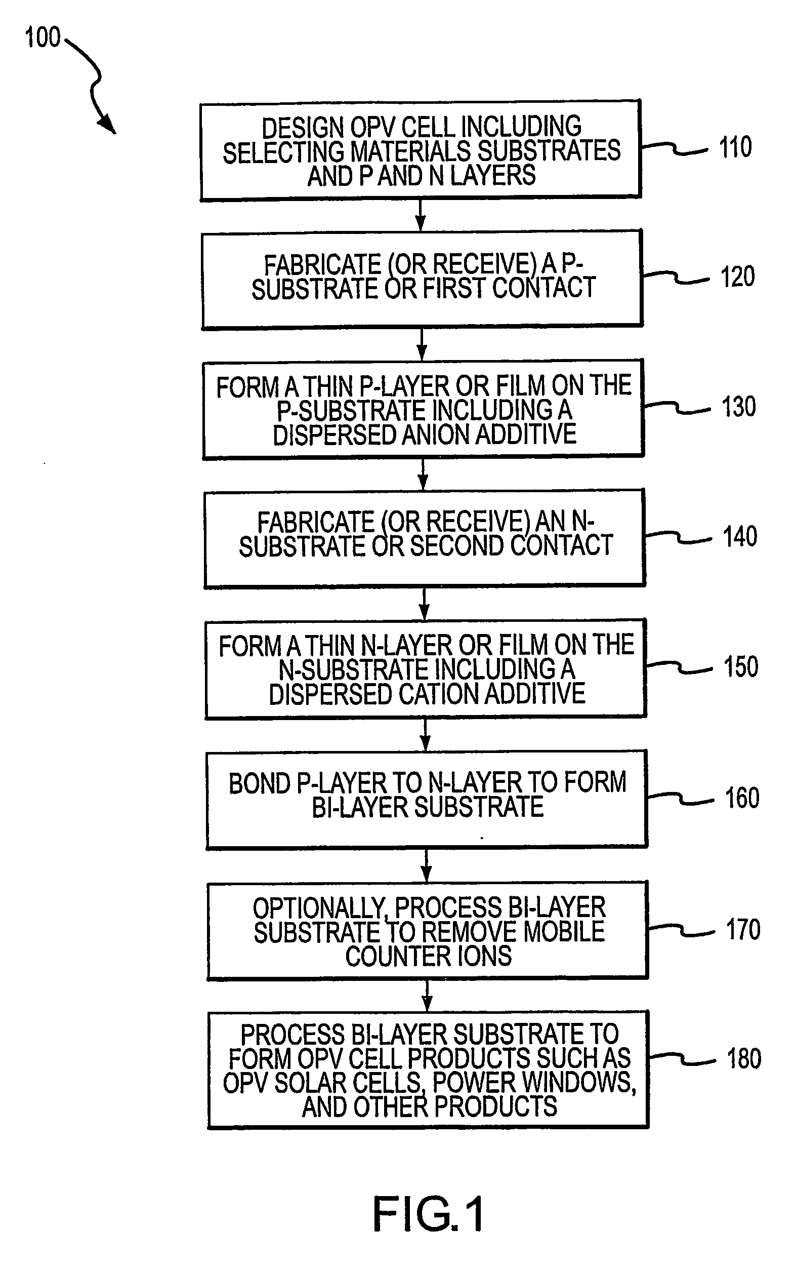
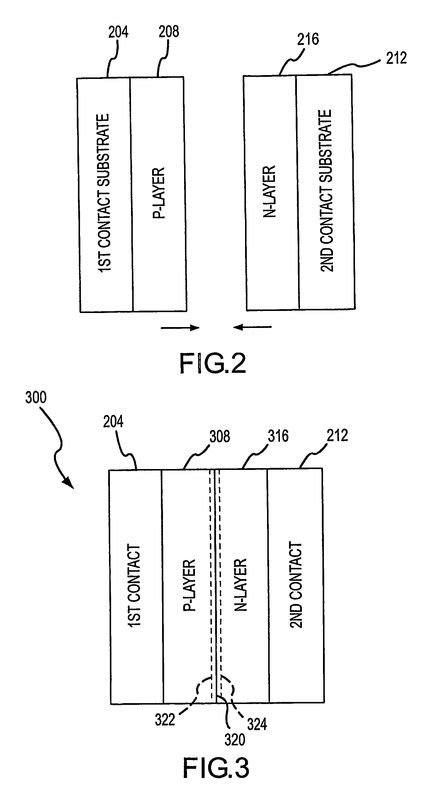
[0023]The present invention is directed generally to a method of fabricating a bi-layer organic photovoltaic (OPV) cell that includes dispersing semiconductor nanocrystals in a binder, such as a polymer binder (e.g., an epoxy) that is applied to conductive substrates to form an n-type substrate and a p-type substrate. The two substrates are then bound together such that there is good adhesion between the n-layer and p-layer and crystals within these layers to form a bi-layer OPV cell with improved efficiency (i.e., up to 5 percent or more whereas existing OPV cells typically have 2 percent or lower efficiencies). As will become clear from the following description, one important aspect of the method of the invention is building an electric field at the p-n heterojunction or interface between the semiconductor films so as to control detrimental recombination which occurs almost solely at this interface. The electric field is provided integral to the OPV cell by covalently binding ion...


PUM

PropertyMeasurementUnit
thicknessesaaaaaaaaaa
thicknessaaaaaaaaaa
sizeaaaaaaaaaa

Abstract

A bi-layer photovoltaic cell, and method (100) of making same, with an electric field applied at the p-n heterojunction interface. The cell includes a first semiconductor layer including a binder, nanocrystals of an n-type semiconductor, and spatially bound cations and a second semiconductor layer contacting the first semiconductor layer that includes a binder, nanocrystals of a p-type semiconductor, and spatially bound anions. The cell further includes a p-n heterojunction at the contacting interface between the first and second semiconductor layers. An electric field is created by the spatially bound cations and anions that are located in the layers proximal to the p-n heterojunction. The nanocrystals are single crystals of organic semiconductors that are less than 50 nanometers in size and that comprise a majority of the volume of their respective layers. The binder is a polymer matrix, such as an epoxy. The cell includes electrical contacts abutting the semiconductor layers.

Description

REFERENCE TO RELATED APPLICATIONS[0001]This application is the National Stage of International Application No. PCT / US04 / 30201, filed Sep. 16, 2004, which claims the benefit under 35 U.S.C. §119(e) of U.S. Provisional Application 60 / 503,336, filed Sep. 16, 2003.TECHNICAL FIELD[0002]The present invention relates generally to photovoltaic cells and semiconductors and their manufacture, and more particularly, to organic photovoltaic cells and methods of manufacturing bi-layer organic photovoltaic cells with improved solar conversion efficiencies achieved by controlling the amount of recombination occurring at the p-n heterojunction or interface between the p-type and n-type semiconductor layers.BACKGROUND ART[0003]The conversion of solar energy into electrical energy is becoming more important as costs and shortages of more standard energy sources continue to increase. Standard solar cells made from inorganic semiconductors, such as silicon cells, have been studied since the 1950s and h...

Claims


Application Information

Patent Timeline
Patent Type & Authority Patents(United States)
IPC IPC(8): H01L31/04H01L31/0256H01L31/0352H01L31/0384H01L31/18H10K99/00
CPCH01L51/0024H01L51/424H01L51/0034H01L51/0035H01L51/0053Y02E10/549H01L2251/308Y10S136/291H01L51/0078Y02P70/50H10K71/50H10K85/10H10K85/111H10K85/621H10K85/311H10K30/20H10K2102/103H10K30/50
Inventor GREGG, BRIAN A
Owner ALLIANCE FOR SUSTAINABLE ENERGY
Learn More