Etch back process approach in dual source plasma reactors

a plasma reactor and etching process technology, applied in the direction of electrical discharge tubes, basic electric elements, electrical apparatus, etc., can solve the problems of frequent operator maintenance, yield loss from non-functional devices, and non-uniform surface with various dimple areas and depths

Inactive Publication Date: 2007-01-09
NOVELLUS SYSTEMS
View PDF11 Cites 20 Cited by
  • Summary
  • Abstract
  • Description
  • Claims
  • Application Information

AI Technical Summary

Benefits of technology

[0009]The invention makes use of a downstream plasma source, which produces a high density of radicals (for example, greater than about 5e13 cm−3) which interact chemically with the substrate surface. The distinguishing feature of a downstream plasma source is that the plasma gases are made to cross a neutralizing barrier, which n

Problems solved by technology

Therefore, a non-uniform surface with various dimple areas and depths will form as a result of the trench and hole features.
A non-uniform film surface can interfere with subsequent IC fabrication steps such as photolithography, film depositions and film removals, and can cause yield loss from non-functional devices.
It is an ongoing challenge for etch back processes to remove the conductive material thoroughly, while leaving a smooth, planar surface, with little or no surface top

Method used


Image

  • Etch back process approach in dual source plasma reactors
  • Etch back process approach in dual source plasma reactors
  • Etch back process approach in dual source plasma reactors

Examples


Embodiment Construction

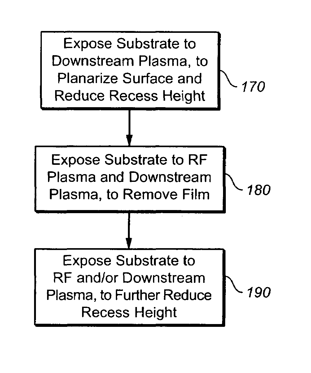
[0019]The novel process is one in which the surface of the substrate is first exposed to a downstream plasma, which serves to reduce the topography on the surface. After planarization, the substrate can be exposed to the normal etching processes, generally including a RF plasma source. By planarizing the film first, the invention avoids the problem wherein the film removal process preserves or enhances existing topography on the substrate surface.

[0020]FIG. 1 illustrates the novel process flow. According to the process flow, the wafer is first exposed 170 to a downstream plasma, to planarize the surface and reduce recess height. The downstream plasma source has the distinguishing feature that the plasma gases are required to cross a neutralizing barrier, which neutralizes through recombination, most of the ionized species in the gas. It has been found that among the effects of a downstream plasma on a substrate, is the general flattening of the topography of the surface. It is hypot...


PUM

PropertyMeasurementUnit
Temperatureaaaaaaaaaa

Abstract

A method is disclosed for removing a polysilicon layer from a semiconductor wafer, in which a downstream plasma source is used first to planarize the wafer, removing contours in the polysilicon layer caused by deposition over lithographic features, such as via holes. The planarizing process is followed by exposure to a plasma made by a direct, radio frequency plasma source, which may be in combination with the downstream plasma source, to perform the bulk etching of the polysilicon. The invention can produce planar surface topography after the top layer of the film is removed, in which the residual recess height of the polysilicon plug filling a via hole is less than about about 10 nm.

Description

FIELD OF THE INVENTION[0001]The present invention relates to a process for making integrated circuit structures. More particularly, this invention relates to processes for removing deposited layers from an integrated circuit structure.BACKGROUND OF THE INVENTION[0002]During various integrated circuit (IC) fabrication steps, numerous layers are deposited onto lower layers which may have previously defined lithographic features such as trenches and holes formed therein. These deposited films often show a conforming surface to the topography of the underlying trenches and holes, as the deposited layers fill in these features. Therefore, a non-uniform surface with various dimple areas and depths will form as a result of the trench and hole features. A non-uniform film surface can interfere with subsequent IC fabrication steps such as photolithography, film depositions and film removals, and can cause yield loss from non-functional devices. Planarization of non-uniform surfaces is theref...

Claims


Application Information

Patent Timeline
IPC IPC(8): H01L21/302
CPCC23F4/00H01J37/32091H01J37/32192H01L21/32137H01J37/32706H01L21/32115H01J37/32357
Inventor CHEN, CINDY W.CHIU, EDDIECHABOYA, MAVIS J.SU, YUH-JIA
Owner NOVELLUS SYSTEMS
Why Eureka
Try Eureka