Process kit for improved power coupling through a workpiece in a semiconductor wafer processing system

Inactive Publication Date: 2007-01-16
APPLIED MATERIALS INC
View PDF24 Cites 10 Cited by
  • Summary
  • Abstract
  • Description
  • Claims
  • Application Information

AI Technical Summary

Benefits of technology

[0011]In sum, the pedestal cover defines a conductive pathway for coupling RF wafer biasing power during wafer processing. By selecting the appropriate frequencies and pedestal cover materials, RF wafer biasing power couples only through the wafer and not through neighboring pedestal components which may exhibit instantaneous conductive characteristics. As such, voltage stability at the wafer and process condition reproducibility is maintained which improves ion deposition from the plasma.

Problems solved by technology

Existing pedestal configurations allow for various electrical paths wherein voltage stability is compromised.
Specifically, stability is compromised due to the hysteresis effect of power coupling through multiple paths to the plasma.
When a ring becomes the momentary path of least resistance, energy losses in the system and voltage instability at the wafer occurs.
The resultant instability of the wafer voltage causes the aforementioned nonuniformity of film deposition on the wafer.
Process repeatability (the ability to duplicate identical process conditions for a large number of individually processed wafers) also suffers as a result of the aforementioned undesirable conditions.

Method used


Image

  • Process kit for improved power coupling through a workpiece in a semiconductor wafer processing system
  • Process kit for improved power coupling through a workpiece in a semiconductor wafer processing system
  • Process kit for improved power coupling through a workpiece in a semiconductor wafer processing system

Examples


Embodiment Construction

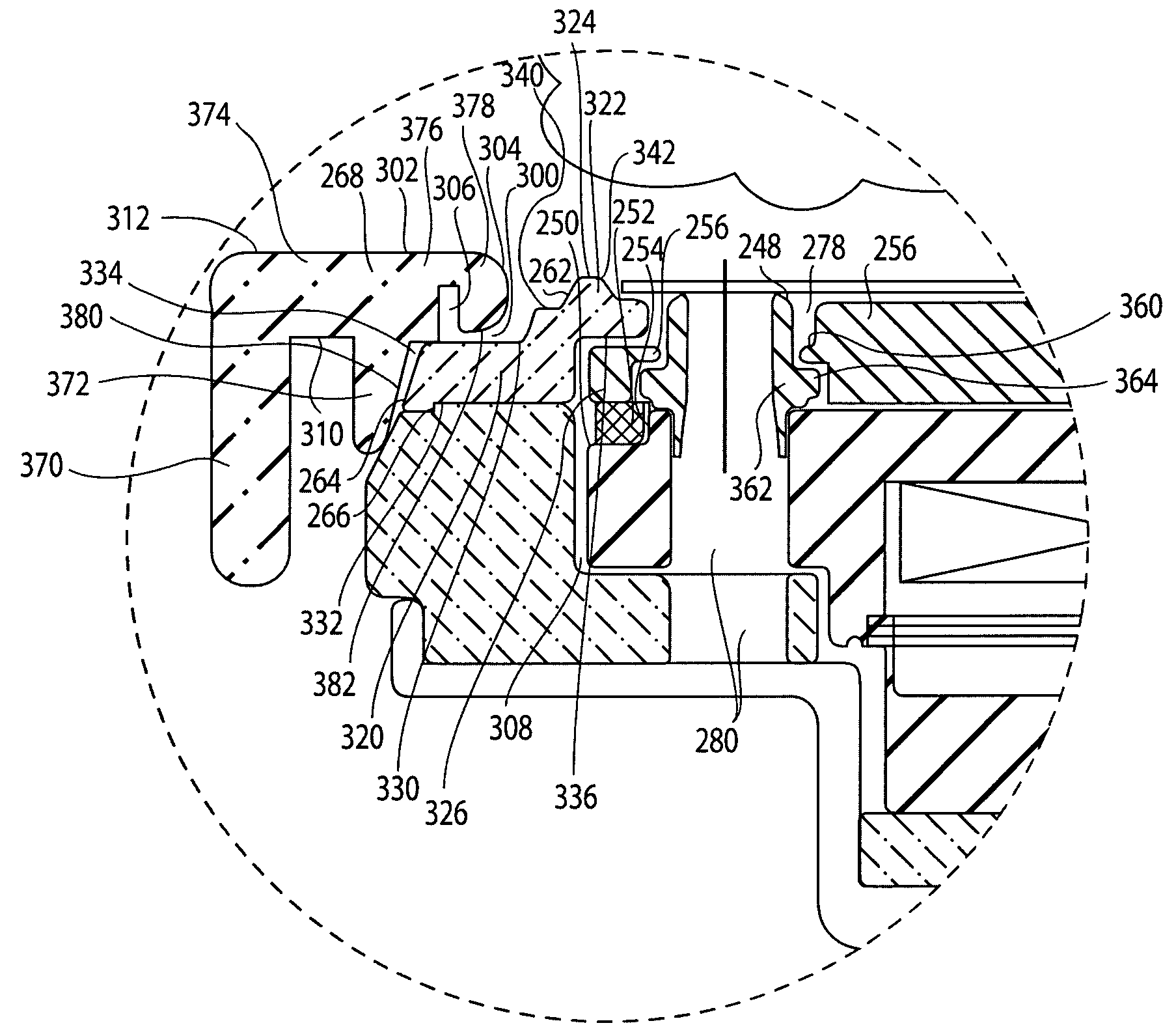
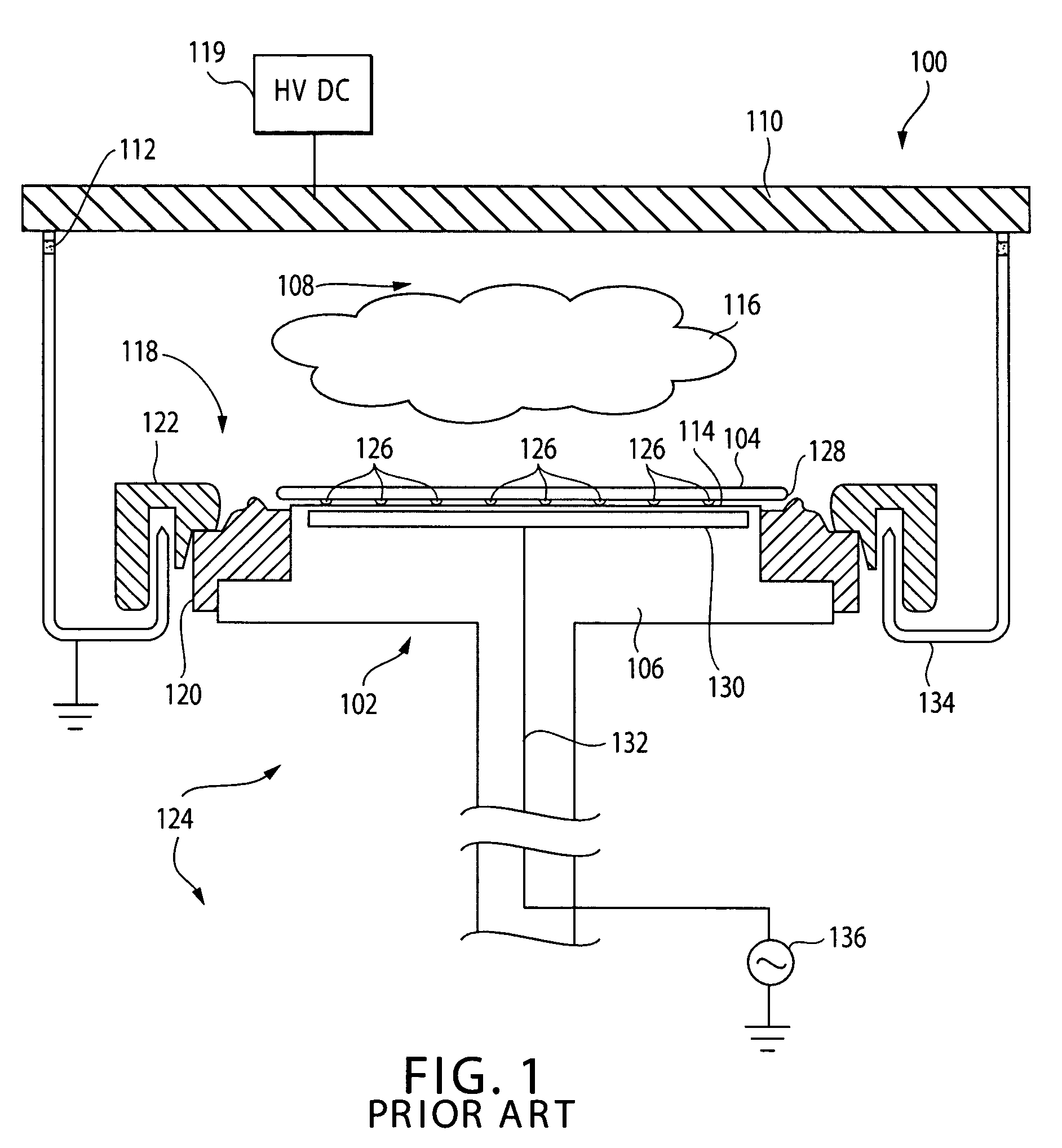
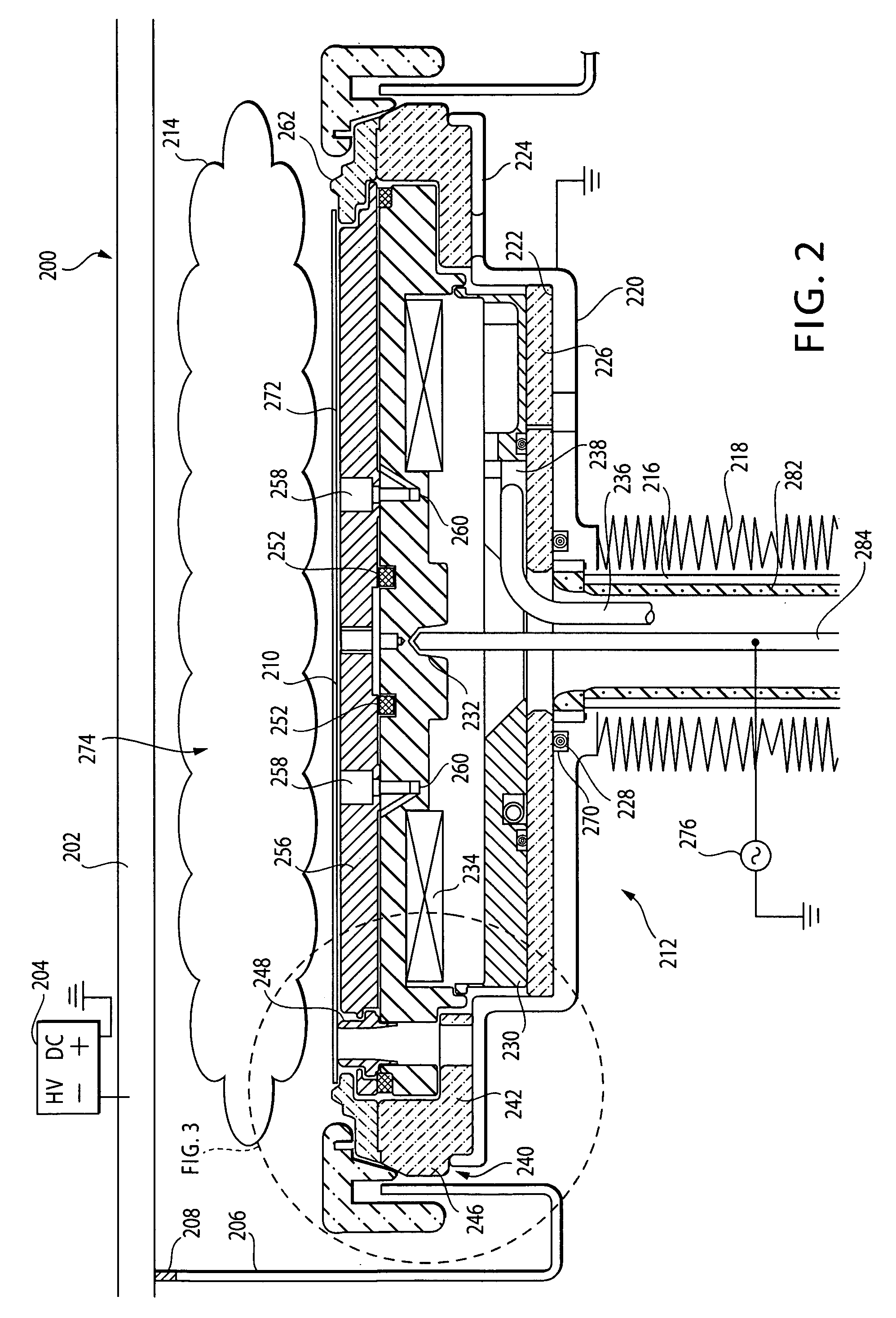
[0018]FIG. 1 depicts a cross-sectional, simplified view of the middle of a conventional PVD wafer processing chamber 100. The chamber 100 contains a conventional pedestal assembly 102 used to support and retain a wafer 104 in the chamber 100. The pedestal assembly 102 comprises a pedestal 106 having a surface 114 that supports the wafer 104. Specifically, the wafer is supported on a disc-like surface having an array of buttons 126 upon which the wafer 104 rests. A chamber lid 110 at the top of the chamber 100 contains deposition target material (e.g., titanium) and is negatively biased by a DC source 119 to form a cathode. Alternately, a separate target is suspended from the chamber lid 110. The chamber lid 110 is electrically insulated from the remainder of the chamber 100 and the chamber 100 is at ground potential. Specifically, insulator ring 112, electrically isolates the chamber lid 110 from a grounded annular shield member 134 which forms an anode.

[0019]An electric field is in...


PUM

PropertyMeasurementUnit
Diameteraaaaaaaaaa

Abstract

Apparatus for supporting a substrate such as a semiconductor wafer in a process chamber to improve power coupling through the substrate. The apparatus contains a pedestal assembly and a pedestal cover positioned over the top surface of and circumscribing the pedestal assembly for electrically isolating the pedestal assembly. The pedestal cover reduces conductive film growth in the wafer process region. As such, RF wafer biasing power from the pedestal assembly remains coupled through the substrate during processing.

Description

CROSS-REFERENCE TO RELATED APPLICATIONS[0001]This application is a continuation of U.S. patent application Ser. No. 10 / 039,907, filed Jan. 2, 2002, now U.S. Pat. No. 6,723,214 which is a continuation of U.S. patent application Ser. No. 09 / 182,023, filed Oct. 29, 1998, now abandoned both of which are incorporated herein by reference.BACKGROUND OF THE INVENTION[0002]1. Field of the Invention[0003]The present invention generally relates to a plasma-enhanced processing of semiconductor wafers and, more specifically, to an apparatus for improving voltage stability on a workpiece and electrical coupling between a plasma and the workpiece in a semiconductor wafer processing system.[0004]2. Description of the Related Art[0005]Plasma-enhanced reactions and processes have become increasingly important to the semiconductor industry, providing for precisely controlled thin-film depositions. For example, a plasma reactor in a high-temperature physical vapor deposition (PVD) semiconductor wafer p...

Claims


Application Information

Patent Timeline
IPC IPC(8): C23C14/34C23C16/00C23C14/50H01J37/32
CPCH01J37/32431H01J37/32
Inventor STIMSON, BRADLEY O.KABURAKI, MITSUHIROFORSTER, JOHN C.DELAURENTIS, ERICGOPALRAJA, PRABURAMRODRIGUEZ, PATRICIASUBRAMANI, ANANTHA
Owner APPLIED MATERIALS INC
Why Eureka
Try Eureka